Altera QDRII SRAM Controller MegaCore Function User Manual
Page 41
Altera Corporation
MegaCore Version 9.1
3–9
November 2009
QDRII SRAM Controller MegaCore Function User Guide
Functional Description
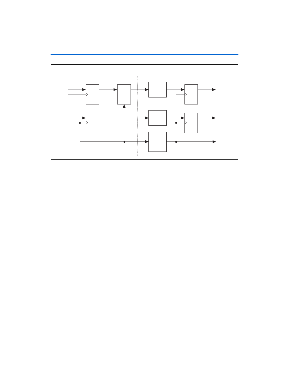
Figure 3–5. Block Diagram of the New Read Capture Implementation
The data from the latch becomes valid following the rising edge of the cq
signal (when the latch becomes transparent) and, in a worst-case
condition, becomes invalid following the rising edge of cqn signal (when
roughly half a cycle = t
KHKH
), which is done by creating a zero-cycle path
between the latch and a device register. The data is re-captured in the
device using the same edge of the cq signal that makes the latch
transparent. Both the cq signal and the data cross the IOE-to-device
boundary where they are delayed. The cq signal is delayed by slightly
more than by the data needed to meet the setup time for this register.
However, the delay is not enough to violate its hold time,which is related
to the rising edge of cqn signal. Because the data is recaptured in the
FPGA while the latch is valid, the IOE capture register timing margins are
not impacted.
is a timing diagram of the IOE that assumes the latch is still
transparent when cqn rising edge occurs. The real B, expected B, and
delayed cq signals represent the data and clock to the re-capture
registers. The output of latch B is either real B or expected B, depending
on the relationship between cq and cqn. To cover both cases, the usable
part of B signal should be captured before going to the resynchronization
FIFO buffers. Routing delay aligns the data with the clock.
I/O
A
B
Fabric
To
FIFO
Buffer
EN
cqn
cq
Latch
Routing
Delay
Routing
Delay
Clock
Network
Delay