Example design, Example design” on – Altera QDRII SRAM Controller MegaCore Function User Manual
Page 59
Altera Corporation
MegaCore Version 9.1
3–27
November 2009
QDRII SRAM Controller MegaCore Function User Guide
Functional Description
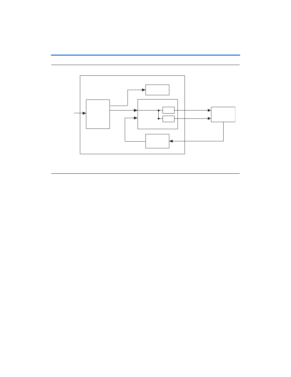
Figure 3–20. PLL Configuration
Notes to
:
(1)
Stratix II devices only.
(2)
Non-DQS mode only.
Example Design
IP Toolbench creates an example design that shows you how to
instantiate and connect up the QDRII SRAM controller. The example
design is a working system that can be compiled and used for both static
timing checks and board tests. It also instantiates an example PLL and
shows you how to generate the external clocks for the QDRII SRAM
device.
The example design consists of the QDRII SRAM controller, some driver
logic to issue read and write requests to the controller, and a PLL to create
the necessary clocks. The asynchronous reset, avl_resetn, drives the
reset logic, which resets the PLL and all the logic. When the PLL is locked
and avl_resetn is deasserted, the reset to the core, soft_reset_n, is
also deasserted. If the PLL lock is lost, the reset logic issues a reset.
shows the testbench and the example design.
Optional
Fed-Back Clock
PLL (Note 2)
FPGA Device
QDRII SRAM
qdrii_k_n
qdrii_k
qdrii_cq
QDRII SRAM
Controller
altddio
clock_source
Enhanced PLL
clk
write_clk
non_dqs_
capture_clock
C0
C1
Stratix II DLL
(Note 1)
altddio