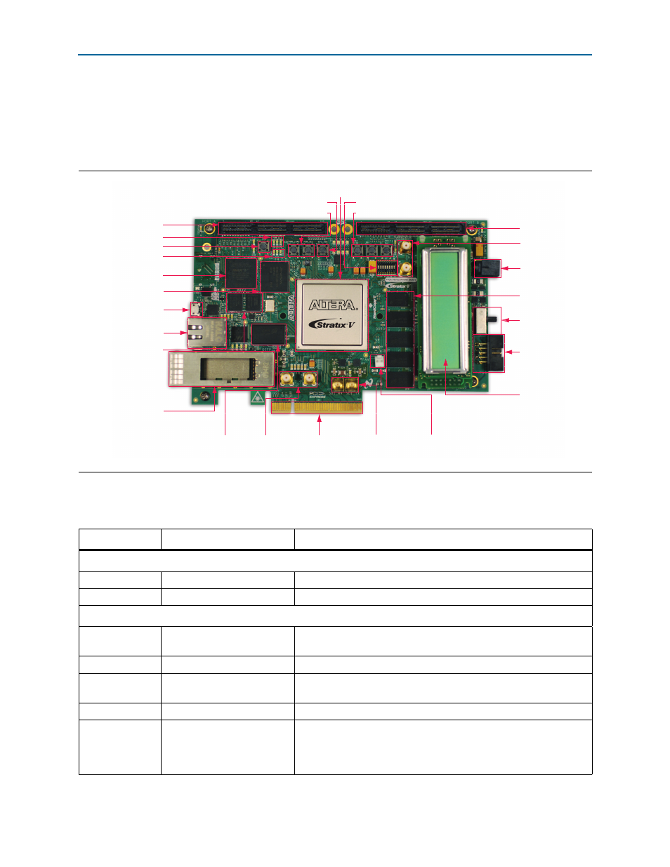
Board overview, Board overview –2, Figure 2–1 – Altera Stratix V GX FPGA Development Board User Manual
Page 10: Table 2–1
2–2
Chapter 2: Board Components
Board Overview
Stratix V GX FPGA Development Board
October 2014
Altera Corporation
Reference Manual
Board Overview
This section provides an overview of the Stratix V GX FPGA development board,
including an annotated board image and component descriptions.
provides an overview of the development board features.
describes the components and lists their corresponding board references.
Figure 2–1. Overview of the Stratix V GX FPGA Development Board Features
HSMC Port B (J2)
Power Switch (SW2)
DC Input Jack (J4)
QDRII+ x18 (U5)
DDR3 Memory
x8 (U12)
x16 (U17, U21, U23, U28)
JTAG Header (J10)
Clock Input
SMA Connector
(J13, J14)
CPU Reset Push Button (S4)
MAX V CPLD
System Controller (U4)
Character LCD (J15)
PCI Express
Edge Connector
(J18)
RLDRAM II x18
Memory
(U20)
Fan Power Header
(J11)
Transceiver TX SMA
Connectors (J3, J6)
Flash x32 Memory
(U10, U11)
Load, Error, Configuration Done
LED (D15-D17)
HSMC Port A (J1)
SDI Video Port
(J16, J17)
Gigabit Ethernet Port (J9)
On-Board USB-Blaster II
Connector (J7)
Program Load, Program Select Push Button (S2, S3)
MAX V Reset Push Button (S1)
Stratix V GX FPGA (U15)
General User Push Button Switches (S5, S6, S7)
User DIP Switch (SW1)
Program Select LED (D4-D6)
40G QSFP Connector
and Cage Assembly (J12)
Table 2–1. Stratix V GX FPGA Development Board Components (Part 1 of 4)
Board Reference
Type
Description
Featured Devices
U15
FPGA
5SGXEA7K2F40C2N, 1517-pin BGA.
U4
CPLD
5M2210ZF256C4, 256-pin BGA.
Configuration, Status, and Setup Elements
J10
JTAG header
Provides access to the JTAG chain by using an external USB-Blaster
cable (disables the on-board USB-Blaster II).
J7
On-Board USB-Blaster II
Micro-USB 2.0 connector for programming and debugging the FPGA.
SW3
JTAG DIP switch
Enables and disables devices in the JTAG chain. This switch is located
on the back of the board.
SW4
FPGA mode select DIP switch
Sets the Stratix V MSEL[4:0] pins.
SW5
Board settings DIP switch
Controls the MAX V CPLD System Controller functions such as clock
select, clock enable, factory or user design load from flash and
FACTORY
signal command sent at power up. This switch is located at
the bottom of the board.