Off-board clock input/output, Off-board clock input/output –25 – Altera Stratix V GX FPGA Development Board User Manual
Page 33
Chapter 2: Board Components
2–25
Clock Circuitry
October 2014
Altera Corporation
Stratix V GX FPGA Development Board
Reference Manual
Off-Board Clock Input/Output
The development board has input and output clocks which can be driven onto the
board. The output clocks can be programmed to different levels and I/O standards
according to the FPGA device’s specification.
lists the clock inputs for the development board.
lists the clock outputs for the development board.
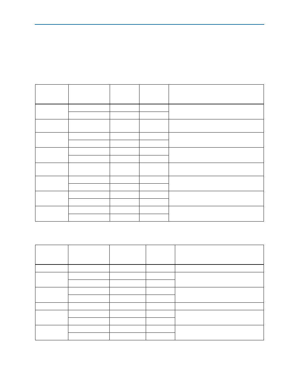
Table 2–23. Off-Board Clock Inputs
Source
Schematic Signal
Name
I/O Standard
Stratix V GX
FPGA Device
Pin Number
Description
SMA
CLKIN_SMA_P
LVPECL
—
Input to LVDS fan-out buffer (drives one REFCLK)
CLKIN_SMA_N
LVPECL
—
Samtec HSMC
HSMA_CLK_IN0
2.5-V
AG28
Single-ended input from the installed HSMC cable
or board.
Samtec HSMC
HSMA_CLK_IN_P1
LVDS/2.5-V
AR8
LVDS input from the installed HSMC cable or
board. Can also support 2x LVTTL inputs.
HSMA_CLK_IN_N1
LVDS/LVTTL
AT8
Samtec HSMC
HSMA_CLK_IN_P2
LVDS/LVTTL
G7
LVDS input from the installed HSMC cable or
board. Can also support 2x LVTTL inputs.
HSMA_CLK_IN_N2
LVDS/LVTTL
G6
Samtec HSMC
HSMB_CLK_IN0
2.5-V
AF29
Single-ended input from the installed HSMC cable
or board.
Samtec HSMC
HSMB_CLK_IN_P1
LVDS/LVTTL
U15
LVDS input from the installed HSMC cable or
board. Can also support 2x LVTTL inputs.
HSMB_CLK_IN_N1
LVDS/LVTTL
T16
Samtec HSMC
HSMB_CLK_IN_P2
LVDS/LVTTL
P16
LVDS input from the installed HSMC cable or
board. Can also support 2x LVTTL inputs.
HSMB_CLK_IN_N2
LVDS/LVTTL
N16
PCI Express
Edge
PCIE_REFCLK_P
LVDS/LVTTL
AF34
LVDS input from the PCI Express edge connector.
PCIE_REFCLK_N
HCSL
AF35
Table 2–24. Off-Board Clock Outputs
Source
Schematic Signal
Name
I/O Standard
Stratix V GX
FPGA Device
Pin Number
Description
Samtec HSMC
HSMA_CLK_OUT0
2.5V CMOS
AJ10
FPGA CMOS output (or GPIO)
Samtec HSMC
HSMA_CLK_OUT_P1
LVDS/2.5V CMOS
AG9
LVDS output. Can also support 2x CMOS
outputs.
HSMA_CLK_OUT_N1
LVDS/2.5V CMOS
AH9
Samtec HSMC
HSMA_CLK_OUT_P2
LVDS/2.5V CMOS
G9
LVDS output. Can also support 2x CMOS
outputs.
HSMA_CLK_OUT_N2
LVDS/2.5V CMOS
G8
Samtec HSMC
HSMB_CLK_OUT0
2.5V CMOS
L16
FPGA CMOS output (or GPIO)
Samtec HSMC
HSMB_CLK_OUT_P1
LVDS/2.5V CMOS
D16
LVDS output. Can also support 2x CMOS
outputs.
HSMB_CLK_OUT_N1
LVDS/2.5V CMOS
C16
Samtec HSMC
HSMB_CLK_OUT_P2
LVDS/2.5V CMOS
B16
LVDS output. Can also support 2x CMOS
outputs.
HSMB_CLK_OUT_N2
LVDS/2.5V CMOS
A16