Altera Stratix V GX FPGA Development Board User Manual
Page 11
Chapter 2: Board Components
2–3
Board Overview
October 2014
Altera Corporation
Stratix V GX FPGA Development Board
Reference Manual
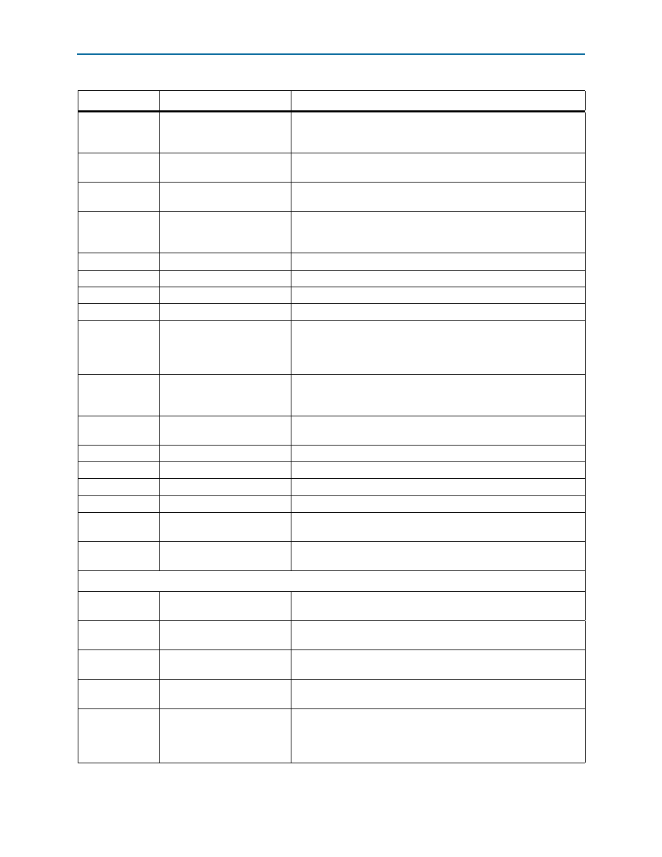
SW6
PCI Express DIP switch
Controls the PCI Express lane width by connecting prsnt pins
together on the PCI Express edge connector. This switch is located at
the back of the board.
S3
Program select push button
Toggles the program LEDs which selects the program image that loads
from flash memory to the FPGA.
S2
Program load push button
Configures the FPGA from flash memory image based on the program
LEDs.
D4, D5, D6
Program LEDs
Illuminates to show the LED sequence that determines which flash
memory image loads to the FPGA when you press the program load
push button.
D17
Configuration done LED
Illuminates when the FPGA is configured.
D15
Load LED
Illuminates during FPGA configuration.
D16
Error LED
Illuminates when the FPGA configuration from flash fails.
D24
Power LED
Illuminates when 5-V power is present.
D25, D26
System Console TX/RX LEDs
Indicate the transmit or receive activity of the System Console USB
interface. The TX and RX LEDs would flicker if the link is in use and
active. The LEDs are either off when not in use or on when in use but
idle.
D27, D28
JTAG TX/RX LEDs
Indicate the transmit or receive activity of the JTAG chain. The TX and
RX LEDs would flicker if the link is in use and active. The LEDs are
either off when not in use or on when in use but idle.
D29, D30, D31,
D32
Ethernet LEDs
Indicate the connection speed as well as transmit or receive activity.
D3, D13
HSMC port A LEDs
You can configure these LEDs to indicate transmit or receive activity.
D1
HSMC port A Present LED
Illuminates when a daughtercard is plugged into the HSMC port A.
D11, D14
HSMC port B LEDs
You can configure these LEDs to indicate transmit or receive activity.
D2
HSMC port B Present LED
Illuminates when a daughtercard is plugged into the HSMC port B.
D33, D34
PCI Express Gen2/Gen3 LED
You can configure these LEDs to illuminate when PCI Express is in
Gen2 or Gen3 mode.
D35, D36, D37
PCI Express Link LEDs
You can configure these LEDs to display the PCI Express link width
(x1, x4, x8).
Clock Circuitry
X1
125 M oscillator
125.000-MHz crystal oscillator for Gigabit Ethernet, Serial RapidIO™
(SRIO), or PCI Express.
U38
Quad-output oscillator
Programmable oscillator with default frequencies of 100 MHz,
156.25 MHz, 625 MHz, and 270 MHz.
U46
Quad-output oscillator
Programmable oscillator with default frequencies of 125 MHz,
644.53125 MHz, 282.5 MHz, and 125 MHz.
X6
148.5 M oscillator
148.500-MHz voltage controlled crystal oscillator for SDI video. This
oscillator is programmable to any frequency between 20-810 MHz.
X4
100 M oscillator
100.000-MHz (programmable to any frequency between 20–810 MHz)
crystal oscillator for PCI Express or general use such as memories.
Multiplex with CLKIN_SMA_P or CLKIN_SMA_N based on CLK_SEL
switch value.
Table 2–1. Stratix V GX FPGA Development Board Components (Part 2 of 4)
Board Reference
Type
Description