Development board block diagram, Handling the board – Altera Stratix V GX FPGA Development Board User Manual
Page 8
1–4
Chapter 1: Overview
Development Board Block Diagram
Stratix V GX FPGA Development Board
October 2014
Altera Corporation
Reference Manual
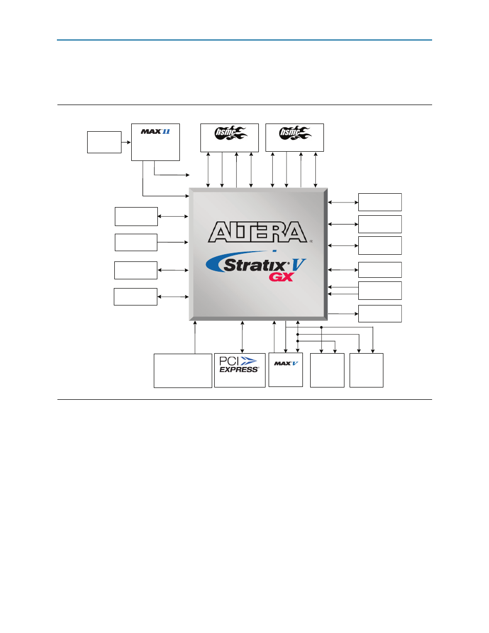
Development Board Block Diagram
shows the block diagram of the Stratix V GX FPGA Development Board.
Handling the Board
When handling the board, it is important to observe the following static discharge
precaution:
c
Without proper anti-static handling, the board can be damaged. Therefore, use
anti-static handling precautions when touching the board.
Figure 1–1. Stratix V GX FPGA Development Board Block Diagram
Port A
Port B
1152 MB
DDR3
4.5 MB
QDRII+ SRAM
Push Buttons
and Switches
LED
CPLD
512 Mb
Flash
512 Mb
Flash
x8 Edge
Programmable
Oscillators
50 MHz, 100 MHz,
148 MHz, 156 MHz
QSFP
REFCLK
SMA IN
GigE
PHY
SDI
TX/TX
On-Board
USB- Blaster II
and USB Interface
x4 XCVR
x1 (LVPECL)
x1
x1 XCVR
x72
x18
72 MB CIO
RLDRAM II
x18
EPCQ
x4
x4
x8
x16
x4
XCVR x8
x32 Config
x32
x80
CLKIN x3
CLKOUT x3
XCVR x8
x80
CLKIN x3
CLKOUT x3
XCVR x6
ADDR
JTAG Chain
5SGXEA7K2F40C2N
Micro-USB
2.0
x19 USB Interface
LVDS/Single-Ended
DQS/Single-Ended
x16
x16