Temperature sense, Temperature sense –60 – Altera Stratix V GX FPGA Development Board User Manual
Page 68
2–60
Chapter 2: Board Components
Temperature Sense
Stratix V GX FPGA Development Board
October 2014
Altera Corporation
Reference Manual
lists the power measurement ADC component references and
manufacturing information.
Temperature Sense
Temperature monitoring for the Stratix V GX FPGA die is achieved with a MAX1619
temperature sense device. The MAX1619 device connects to the MAX V CPLD
EPM2210 System Controller and the Stratix V GX FPGA device by a 2-wire SMB
interface. The MAX1619 device is located at address 0x1. This bus is also routed to a
single voltage and power monitor chip for the 12-V power rail at address 0x2.
The OVERTEMPn and TSENSE_ALERTn signals are driven by the MAX1619 temperature
sense device based on a programmable threshold temperature. The OVERTEMPn signal
is driven to the MAX V System Controller, which controls the OVERTEMPn signal. The
MAX V System Controller can control fan speed based on a register setting and can
also override the MAX1619 device. For more information on this control, refer to the
MAX V System Controller source code found in the development board installation
directory <install dir>\stratixV_GX_fpga\examples\max.
f
For more information on the development board installation directory, refer to the
.
The remote sense routes to the FPGA's diode pins to measure the voltage drop. For
very accurate temperature readings, the I/O adjacent to the FPGA diode sense pins
must be halted.
5
S5_VCC_1p5
1.5
VCCD_FPLL
PLL digital power
VCCH_GXB
XCVR block level transmit buffers
VCCPT
Programmable power tech auxiliary
6
S5_VCCIO_2.5V
2.5
VCCIO_3A
I/O supply bank 3A
VCCIO_3B
I/O supply bank 3B
VCCIO_4B
I/O supply bank 4B (HSMC Port A)
VCCIO_7B
I/O supply bank 7B (HSMC Port A)
7
S5_VCCIO_1.5V
1.5
VCCIO_8A
I/O supply bank 8A (DDR3 RZQ)
VCCIO_8B
I/O supply bank 8B (DDR3)
VCCIO_8C
I/O supply bank 8C (DDR3)
VCCIO_8D
I/O supply bank 8D (DDR3)
8
S5_VCCA_GXB
3.3
VCCA_GXB
XCVR TX driver, RX receiver, CDR
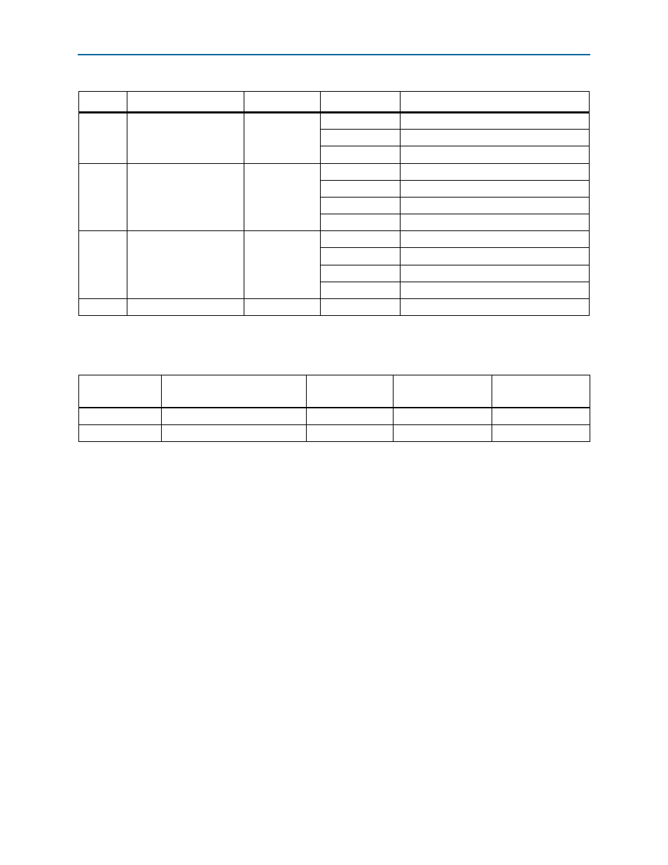
Table 2–59. Power Rail Measurements Based on the GUI Selection (Part 2 of 2)
Number
Schematic Signal Name
Voltage (V)
Device Pin
Description
Table 2–60. Power Measurement ADC Component References and Manufacturing Information
Board Reference
Description
Manufacturer
Manufacturing
Part Number
Manufacturer
Website
U52
8-channel differential 24-bit ADC
Linear Technology
LTC2418CGN#PBF
U1
1-channel differential 14-bit ADC
Linear Technology
LTC2990IMS#PBF