Altera Stratix V GX FPGA Development Board User Manual
Page 12
2–4
Chapter 2: Board Components
Board Overview
Stratix V GX FPGA Development Board
October 2014
Altera Corporation
Reference Manual
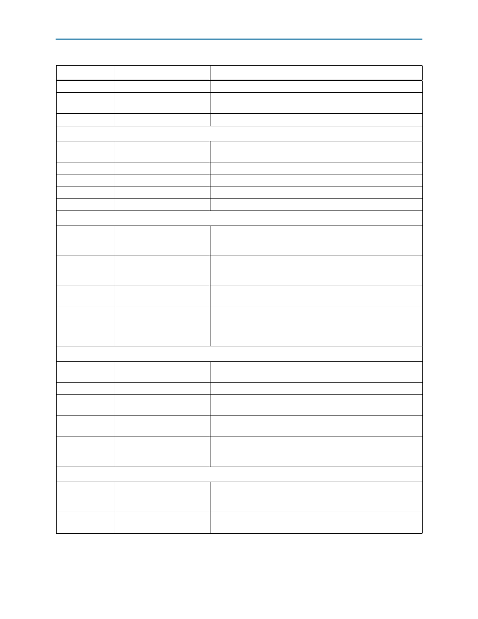
X3
50 M oscillator
50.000-MHz crystal oscillator for general purpose logic.
J13, J14
Clock input SMAs
Drives LVPECL-compatible clock inputs into the clock multiplexer
buffer.
U4
100 M oscillator
100-MHz crystal oscillator for the MAX V CPLD System Controller.
General User Input and Output
D7-D10,
D18-D21
User LEDs
Eight bi-color LEDs (green and red) for 16 user LEDs. Illuminates when
driven low.
SW1
User DIP switch
Octal user DIP switches. When the switch is ON, a logic 0 is selected.
S1
MAX V reset push button
The default reset for the MAX V CPLD System Controller.
S4
CPU reset push button
The default reset for the FPGA logic.
S5, S6, S7
General user push button
Three user push buttons. Driven low when pressed.
Memory Devices
U12, U17, U21,
U23, U28
DDR3 x72
A 1152-MB DDR3 SDRAM with a 72-bit data bus. The 72-bit data bus
consists of four x16 devices and one x8 device with a single address or
command bus.
U5
QDRII+ x18
A 4.5-MB QDRII+ SRAM with a 18-bit data bus. The device has a
separate 18-bit read and 18-bit write port with DDR signalling at up to
550 MHz.
U20
RLDRAM II x18
A 72-MB CIO RLDRAM II with a 18-bit data bus. The 18-bit data bus
consists of a single x18 device with a single address or command bus.
U10, U11
Flash x32
Two 512-Mb synchronous flash devices with a 16-bit data buses for
non-volatile memory. The board supports two flash devices of 16-bit
interface each, which combine to allow for 1-Gbyte (GB) synchronous
flash with a 32-bit data bus.
Communication Ports
J18
PCI Express edge connector
Made of gold-plated edge fingers for up to ×8 signaling in either Gen1,
Gen2, or Gen3 mode.
J12
QSFP connector
Provides four transceiver channels for a 40G QSFP module.
J1
HSMC port A
Provides eight transceiver channels and 84 CMOS or 17 LVDS
channels per the HSMC specification.
J2
HSMC port B
Provides four transceiver channels and 84 CMOS or a DQ/DQS
interface.
J9
Gigabit Ethernet port
RJ-45 connector which provides a 10/100/1000 Ethernet connection
via a Marvell 88E1111 PHY and the FPGA-based Altera Triple Speed
Ethernet MAC MegaCore function in SGMII mode.
Video and Display Ports
J16, J17
SDI video port
Two 75-
system management bus (SMB) connectors which provide a
full-duplex SDI interface through a LMH0303 driver and LMH0384
cable equalizer.
J15
Character LCD header
A single 14-pin 0.1" pitch dual-row header which interfaces to the 16
character × 2 line LCD module.
Table 2–1. Stratix V GX FPGA Development Board Components (Part 3 of 4)
Board Reference
Type
Description