Altera Stratix V GX FPGA Development Board User Manual
Page 40
2–32
Chapter 2: Board Components
Components and Interfaces
Stratix V GX FPGA Development Board
October 2014
Altera Corporation
Reference Manual
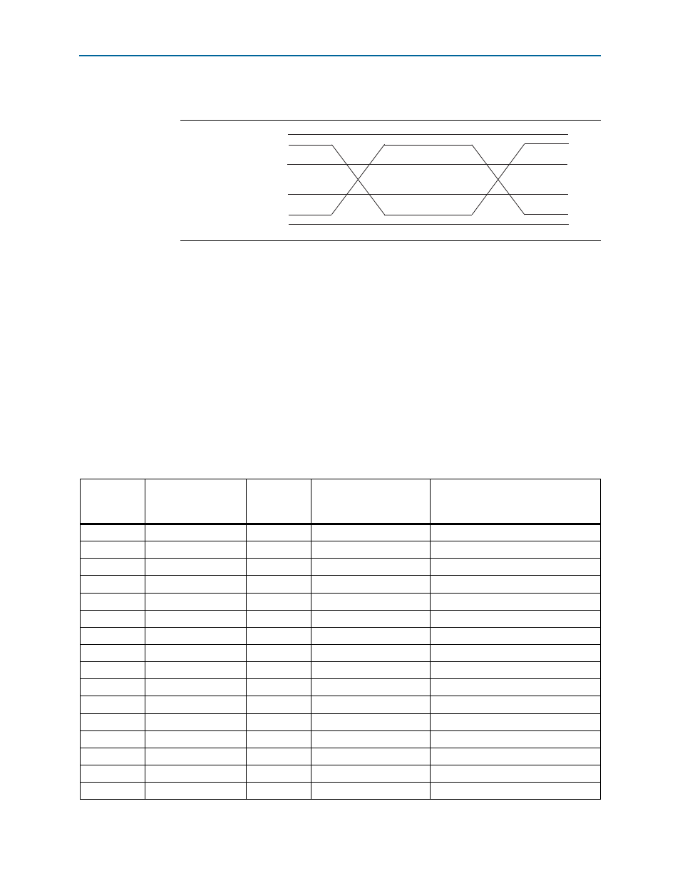
shows the PCI Express reference clock levels.
The SMB and JTAG are optional signals in the PCI Express specification. The SMB
signals are wired to the Stratix V GX FPGA device and the JTAG signals control the
JTAG chain if enabled by the JTAG control DIP switch (SW3.4). The PCI Express
control DIP switch allows the presence detect grounding to be altered to enable a ×1,
×4, or ×8 width edge connector. The PCI Express control DIP switch does not support
auto-negotiation.
The PCI Express edge connector also has a presence detect feature for the
motherboard to determine if a card is installed. A jumper is provided to optionally
connect PRSNT1n to any of the three PRSNT2n pins found within the x8 connector
definition. This is to address issues on some PC systems that would base the
link-width capability on the presence detect pins versus a query operation.
summarizes the PCI Express pin assignments. The signal names and
directions are relative to the Stratix V GX FPGA.
Figure 2–6. PCI Express Reference Clock Levels
V
MAX
= 1.15 V
V
CROSS MAX
= 550 mV
V
CROSS MIN
= 250 mV
V
MIN
= –0.30 V
REFCLK –
REFCLK +
Table 2–37. PCI Express Pin Assignments, Schematic Signal Names, and Functions (Part 1 of 2)
Board
Reference
(J18)
Schematic Signal
Name
I/O Standard
Stratix V GX FPGA Device
Pin Number
Description
B14
PCIE_RX_P0
1.4-V PCML
AV38
Receive bus
B15
PCIE_RX_N0
1.4-V PCML
AV39
Receive bus
B19
PCIE_RX_P1
1.4-V PCML
AT38
Receive bus
B20
PCIE_RX_N1
1.4-V PCML
AT39
Receive bus
B23
PCIE_RX_P2
1.4-V PCML
AP38
Receive bus
B24
PCIE_RX_N2
1.4-V PCML
AP39
Receive bus
B27
PCIE_RX_P3
1.4-V PCML
AM38
Receive bus
B28
PCIE_RX_N3
1.4-V PCML
AM39
Receive bus
B33
PCIE_RX_P4
1.4-V PCML
AH38
Receive bus
B34
PCIE_RX_N4
1.4-V PCML
AH39
Receive bus
B37
PCIE_RX_P5
1.4-V PCML
AF38
Receive bus
B38
PCIE_RX_N5
1.4-V PCML
AF39
Receive bus
B41
PCIE_RX_P6
1.4-V PCML
AD38
Receive bus
B42
PCIE_RX_N6
1.4-V PCML
AD39
Receive bus
B45
PCIE_RX_P7
1.4-V PCML
AB38
Receive bus
B46
PCIE_RX_N7
1.4-V PCML
AB39
Receive bus