Altera Stratix V GX FPGA Development Board User Manual
Page 22
2–14
Chapter 2: Board Components
Configuration, Status, and Setup Elements
Stratix V GX FPGA Development Board
October 2014
Altera Corporation
Reference Manual
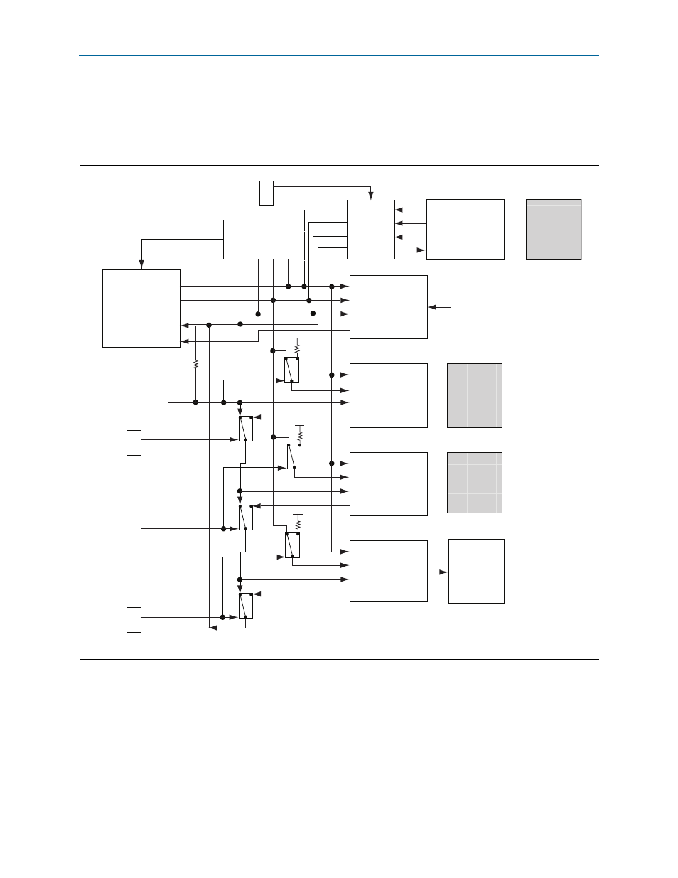
JTAG Chain
The on-board USB-Blaster II is automatically disabled when you connect an external
USB-Blaster to the JTAG chain or when you enable JTAG from the PCI Express edge
connector.
illustrates the JTAG chain.
Each jumper shown in
is located in the JTAG DIP switch (SW3) on the back
of the board. To connect a device or interface in the chain, their corresponding switch
must be in the OFF position. Push all the switches in the ON position to only have the
FPGA in the chain. Note that the MAX V CPLD System Controller must be in the
chain to use some of the GUI interfaces.
Figure 2–3. JTAG Chain
Cypress
On-Board
USB-Blaster II
GPIO
TCK
Stratix V GX
FPGA
Analog
Switch
MAX V
System
Controller
HSMC
Port A
HSMC
Port B
GPIO
TMS
GPIO
TDO
GPIO
TDI
JTAG Master
GPIO
DISABLE
ENABLE
ENABLE
ENABLE
ENABLE
JTAG Slave
JTAG Slave
Installed
HSMC
Card
Installed
HSMC
Card
TCK
TMS
TDI
TDO
TCK
2.5 V
TMS
TDI
TDO
TCK
TMS
TDI
TDO
TCK
TMS
TDI
TDO
JTAG Slave
JTAG Slave
Analog
Switch
Analog
Switch
ALWAYS
ENABLED
(in chain)
DIP Switch
DIP Switch
DIP Switch
DIP Switch
10-pin
JTAG Header
Flash
Memory
PCI Express
Edge
Connector
JTAG Master
PCI Express
Motherboard
TCK
TMS
TDI
TDO
Level
Translator
2.5 V
2.5 V