Sdi video output/input, Sdi video output/input –43 – Altera Stratix V GX FPGA Development Board User Manual
Page 51
Chapter 2: Board Components
2–43
Components and Interfaces
October 2014
Altera Corporation
Stratix V GX FPGA Development Board
Reference Manual
lists the HSMC connector component reference and manufacturing
information.
SDI Video Output/Input
The serial digital interface (SDI) video port consists of a LMH0303 cable driver and a
LMH0384 receiver cable equalizer. The PHY devices from National Semiconductor
interface to single-ended 75- SMB connectors.
The cable driver supports operation at 270 Mbit standard definition (SD), 1.5 Gbit
high definition (HD), and 3.0 Gbit dual-link HD modes. Control signals are allowed
for SD and HD modes selections, as well as device enable. The device can be clocked
by the 148.5 MHz voltage-controlled crystal oscillator (VCXO) and matched to
incoming signals within 50 ppm using the UP and DN voltage control lines to the
VCXO.
shows the supported output standards for the SD and HD input.
f
For more information about the application circuit of the LMH0303 cable driver, refer
to the cable driver data sheet at
summarizes the SDI video output interface pin assignments, signal names,
and functions.
The cable equalizer supports operation at 270 Mbit SD, 1.5 Gbit HD, and 3.0 Gbit
dual-link HD modes. Control signals are allowed for bypassing or disabling the
device, as well as a carrier detect or auto-mute signal interface.
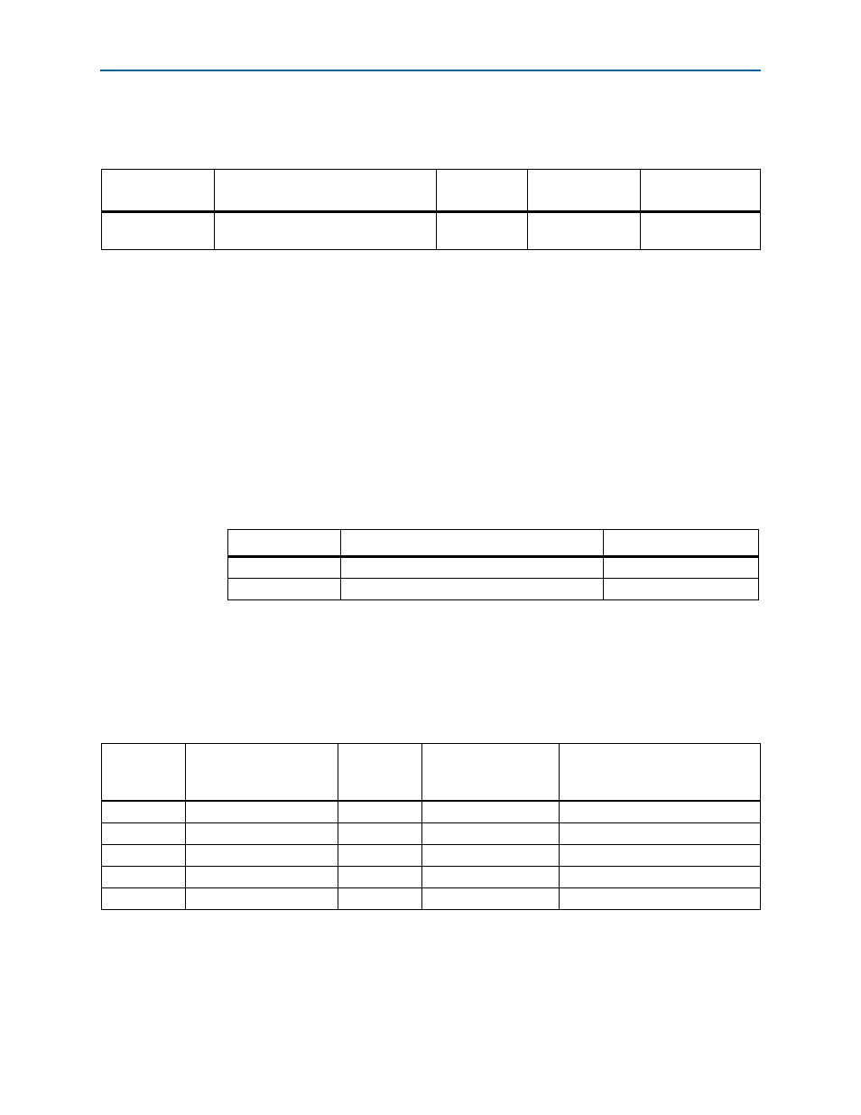
Table 2–42. HSMC Connector Component Reference and Manufacturing Information
Board Reference
Description
Manufacturer
Manufacturing
Part Number
Manufacturer
Website
J1 and J2
HSMC, custom version of QSH-DP
family high-speed socket.
Samtec
ASP-122953-01
Table 2–43. Supported Output Standards for SD and HD Input
SD_HD Input
Supported Output Standards
Rise TIme
0
SMPTE 424M, SMPTE 292M
Faster
1
SMPTE 259M
Slower
Table 2–44. SDI Video Output Interface Pin Assignments, Schematic Signal Names, and Functions
Board
Reference
(U25)
Schematic
Signal Name
I/O Standard
Stratix V GX FPGA
Device
Pin Number
Description
6
SDI_TX_EN
2.5-V
AK27
Device enable
4
SDI_TX_RSET
3.3-V
—
Device reset
10
SDI_TX_SD_HDn
2.5-V
AJ27
High definition select
1
SDI_TX_P
1.4-V PCML
E36
SDI video input P
2
SDI_TX_N
1.4-V PCML
E37
SDI video input N