Altera Stratix V GX FPGA Development Board User Manual
Page 59
Chapter 2: Board Components
2–51
Memory
October 2014
Altera Corporation
Stratix V GX FPGA Development Board
Reference Manual
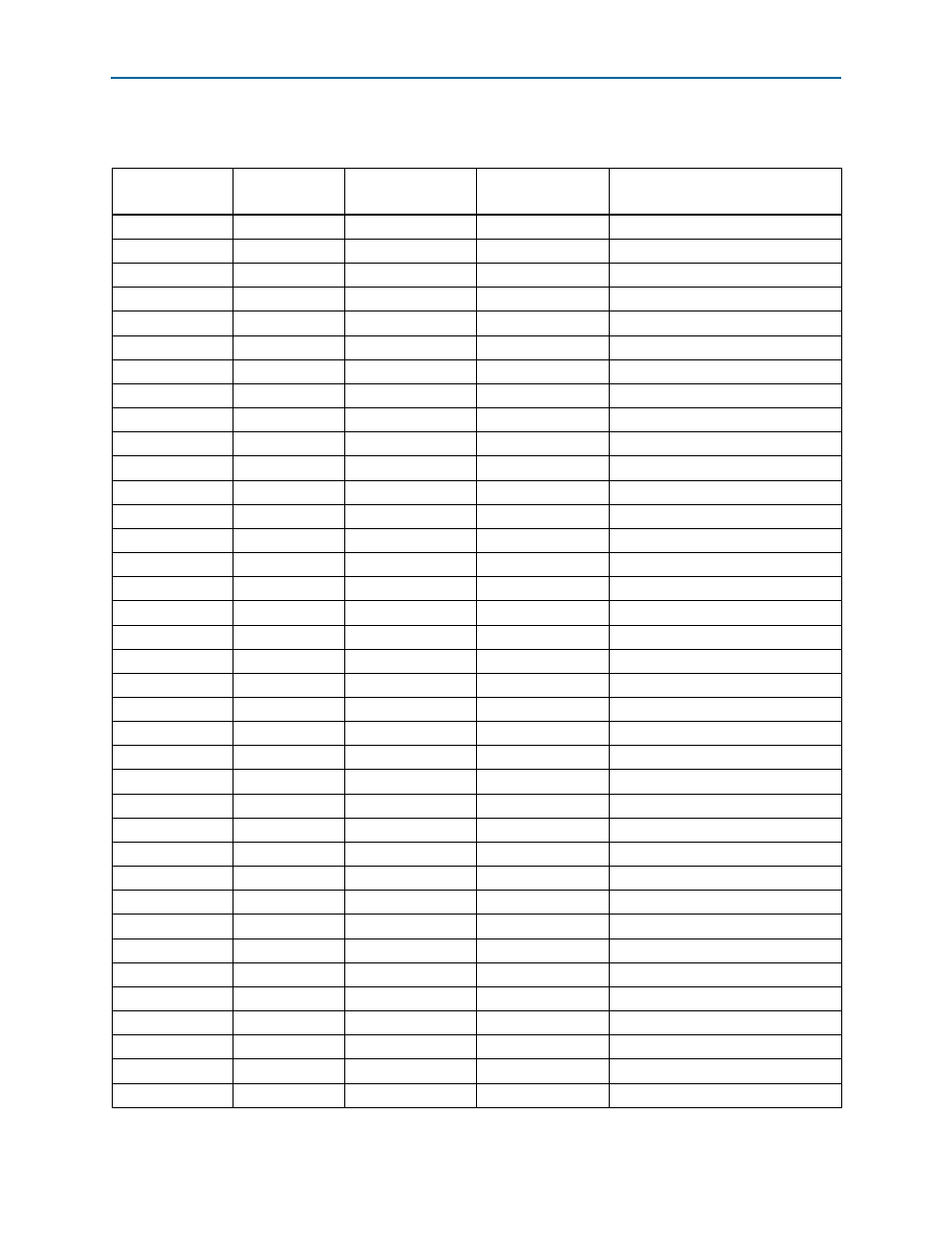
lists the QDRII+ pin assignments, signal names, and functions.
Table 2–52. QDRII+ Pin Assignments, Signal Names and Functions (Part 1 of 2)
Board Reference
(U5)
Schematic
Signal Name
I/O Standard
Stratix V GX FPGA
Device Pin Number
Description
A2
QDRII_A20
1.8-V HSTL Class I
AA13
Address bus (reserved for 144M)
A10
QDRII_A19
1.8-V HSTL Class I
AP12
Address bus (reserved for 72M)
A3
QDRII_A18
1.8-V HSTL Class I
AA12
Address bus
A9
QDRII_A17
1.8-V HSTL Class I
AN12
Address bus
R7
QDRII_A16
1.8-V HSTL Class I
AL13
Address bus
R5
QDRII_A15
1.8-V HSTL Class I
AF14
Address bus
R4
QDRII_A14
1.8-V HSTL Class I
AC13
Address bus
R3
QDRII_A13
1.8-V HSTL Class I
AB13
Address bus
P8
QDRII_A12
1.8-V HSTL Class I
AW14
Address bus
P7
QDRII_A11
1.8-V HSTL Class I
AM13
Address bus
P5
QDRII_A10
1.8-V HSTL Class I
AE14
Address bus
P4
QDRII_A9
1.8-V HSTL Class I
AC14
Address bus
N7
QDRII_A8
1.8-V HSTL Class I
AJ13
Address bus
N6
QDRII_A7
1.8-V HSTL Class I
AH13
Address bus
N5
QDRII_A6
1.8-V HSTL Class I
AD14
Address bus
C7
QDRII_A5
1.8-V HSTL Class I
AN13
Address bus
C5
QDRII_A4
1.8-V HSTL Class I
AG13
Address bus
B8
QDRII_A3
1.8-V HSTL Class I
AT14
Address bus
B4
QDRII_A2
1.8-V HSTL Class I
AF13
Address bus
R8
QDRII_A1
1.8-V HSTL Class I
AP13
Address bus
R9
QDRII_A0
1.8-V HSTL Class I
AU14
Address bus
N2
QDRII_D17
1.8-V HSTL Class I
AU15
Write data bus
M3
QDRII_D16
1.8-V HSTL Class I
AR15
Write data bus
L3
QDRII_D15
1.8-V HSTL Class I
AR14
Write data bus
J3
QDRII_D14
1.8-V HSTL Class I
AP15
Write data bus
G2
QDRII_D13
1.8-V HSTL Class I
AT15
Write data bus
F3
QDRII_D12
1.8-V HSTL Class I
AN14
Write data bus
D2
QDRII_D11
1.8-V HSTL Class I
AN15
Write data bus
C3
QDRII_D10
1.8-V HSTL Class I
AM14
Write data bus
B3
QDRII_D9
1.8-V HSTL Class I
AL15
Write data bus
C11
QDRII_D8
1.8-V HSTL Class I
AG14
Write data bus
D11
QDRII_D7
1.8-V HSTL Class I
AD16
Write data bus
E10
QDRII_D6
1.8-V HSTL Class I
AE15
Write data bus
G11
QDRII_D5
1.8-V HSTL Class I
AA14
Write data bus
J11
QDRII_D4
1.8-V HSTL Class I
AA15
Write data bus
K10
QDRII_D3
1.8-V HSTL Class I
AC15
Write data bus
M11
QDRII_D2
1.8-V HSTL Class I
AB15
Write data bus