Altera Stratix V GX FPGA Development Board User Manual
Page 16
2–8
Chapter 2: Board Components
MAX V CPLD System Controller
Stratix V GX FPGA Development Board
October 2014
Altera Corporation
Reference Manual
FACTORY_STATUS
N12
—
1.8-V
On-Board USB-Blaster II FACTORY command
status
FLASH_ADVn
N7
AP7
1.8-V
FM bus flash memory address valid
FLASH_CEn0
R5
AV14
1.8-V
FM bus flash memory chip enable 0
FLASH_CEn1
M7
AW13
1.8-V
FM bus flash memory chip enable 1
FLASH_CLK
R6
AM8
1.8-V
FM bus flash memory clock
FLASH_OEn
M6
AJ7
1.8-V
FM bus flash memory output enable
FLASH_RDYBSYN0
T5
AL6
1.8-V
FM bus flash memory chip ready 0
FLASH_RDYBSYN1
R7
AN7
1.8-V
FM bus flash memory chip ready 1
FLASH_RESETn
P7
AJ6
1.8-V
FM bus flash memory reset
FLASH_WEn
N6
AN8
1.8-V
FM bus flash memory write enable
FM_A0
E14
AW19
1.8-V
FM address bus
FM_A1
C14
AV19
1.8-V
FM address bus
FM_A2
C15
AM16
1.8-V
FM address bus
FM_A3
E13
AL16
1.8-V
FM address bus
FM_A4
E12
AF16
1.8-V
FM address bus
FM_A5
D15
AG16
1.8-V
FM address bus
FM_A6
F14
AN17
1.8-V
FM address bus
FM_A7
D16
AM17
1.8-V
FM address bus
FM_A8
F13
AP16
1.8-V
FM address bus
FM_A9
E15
AN16
1.8-V
FM address bus
FM_A10
E16
AT17
1.8-V
FM address bus
FM_A11
F15
AR17
1.8-V
FM address bus
FM_A12
G14
AU16
1.8-V
FM address bus
FM_A13
F16
AU17
1.8-V
FM address bus
FM_A14
G13
AW16
1.8-V
FM address bus
FM_A15
G15
AV16
1.8-V
FM address bus
FM_A16
G12
AW17
1.8-V
FM address bus
FM_A17
G16
AV17
1.8-V
FM address bus
FM_A18
H14
AU6
1.8-V
FM address bus
FM_A19
H15
AT6
1.8-V
FM address bus
FM_A20
H13
AL17
1.8-V
FM address bus
FM_A21
H16
AK17
1.8-V
FM address bus
FM_A22
J13
AE16
1.8-V
FM address bus
FM_A23
R3
AE17
1.8-V
FM address bus
FM_A24
P5
AH16
1.8-V
FM address bus
FM_A25
T2
AP21
1.8-V
FM address bus
FM_D0
J14
AN21
1.8-V
FM data bus
FM_D1
J15
AD21
1.8-V
FM data bus
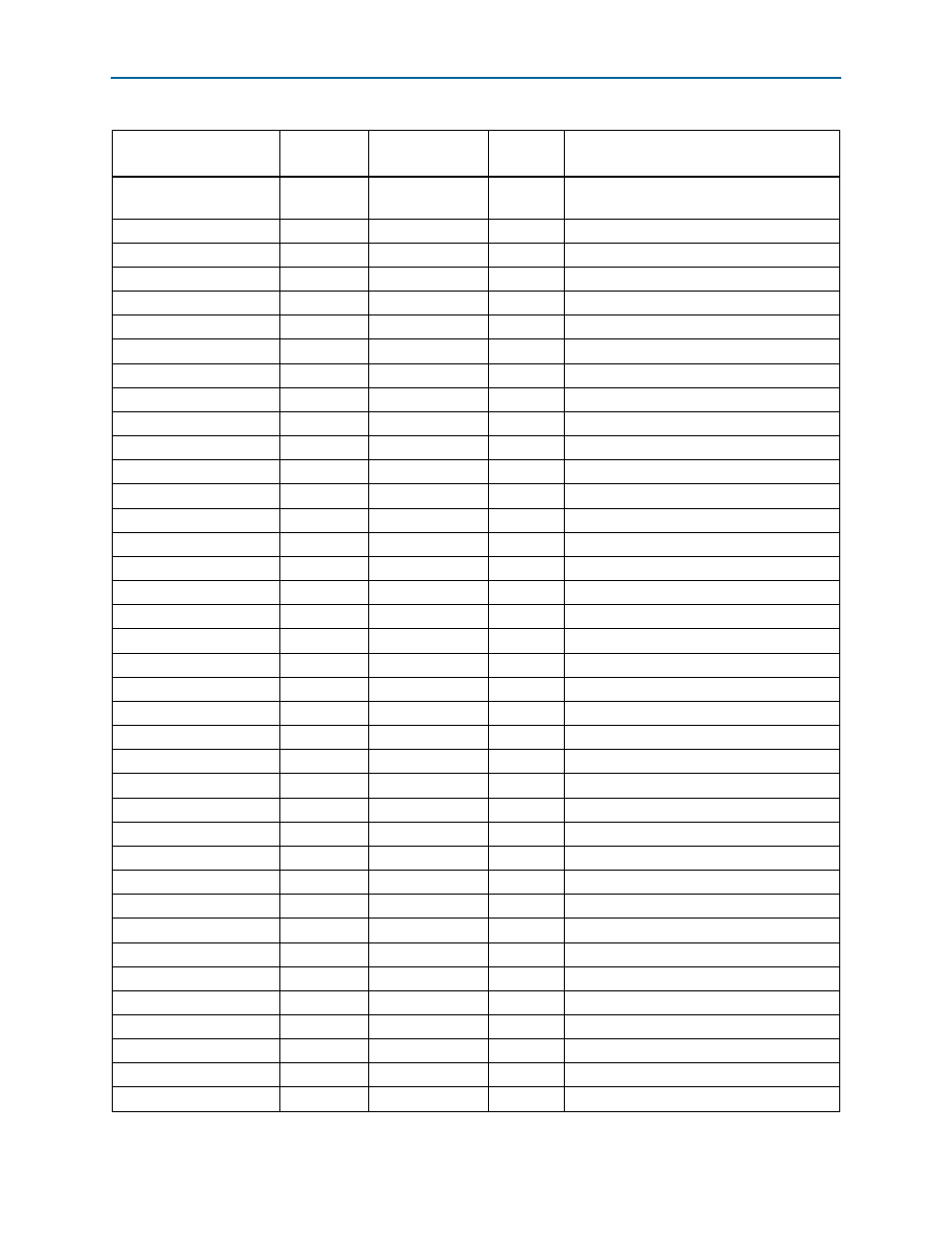
Table 2–5. MAX V CPLD System Controller Device Pin-Out (Part 2 of 6)
Schematic Signal Name
MAX V CPLD
Pin Number
Stratix V GX FPGA
Pin Number
I/O
Standard
Description