Altera Stratix V GX FPGA Development Board User Manual
Page 52
2–44
Chapter 2: Board Components
Components and Interfaces
Stratix V GX FPGA Development Board
October 2014
Altera Corporation
Reference Manual
shows the cable equalizer lengths.
is an excerpt from the LMH0384 cable equalizer data sheet which shows
the SDI cable equalizer.
summarizes the SDI video input interface pin assignments, signal names,
and functions.
Table 2–45. SDI Cable Equalizer Lengths
Data Rate (Mbps)
Cable Type
Maximum Cable Length (m)
270
Belden 1694A
400
1485
140
2970
120
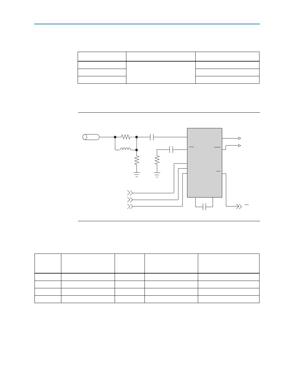
Figure 2–9. SDI Cable Equalizer
BYPASS
MUTE
REF
1.0
μF
75
Ω
37.4
Ω
1.0
μF
1.0
μF
CD
SDI
SDI
SDO
SDO
CD
MUTE
MUTE
REF
BYPASS
AEC+
AEC–
75
Ω
MUTE
Coaxial Cable
SDI Adaptive
Cable Equalizer
To FPGA
3.9 nH
Table 2–46. SDI Video Input Interface Pin Assignments, Schematic Signal Names, and Functions
Board
Reference
(U24)
Schematic
Signal Name
I/O Standard
Stratix V GX FPGA Device
Pin Number
Description
7
SDI_RX_BYPASS
2.5-V
AB30
Equalizer bypass enable
14
SDI_RX_EN
2.5-V
AB28
Device enable
11
SDI_RX_P
1.4-V PCML
F38
SDI video output P
10
SDI_RX_N
1.4-V PCML
F39
SDI video output N