Figure 2–1 – Altera SDI HSMC User Manual
Page 10
2–2
Chapter 2: Board Components
Board Overview
© July 2009 Altera Corporation
shows the bottom view of the SDI HSMC.
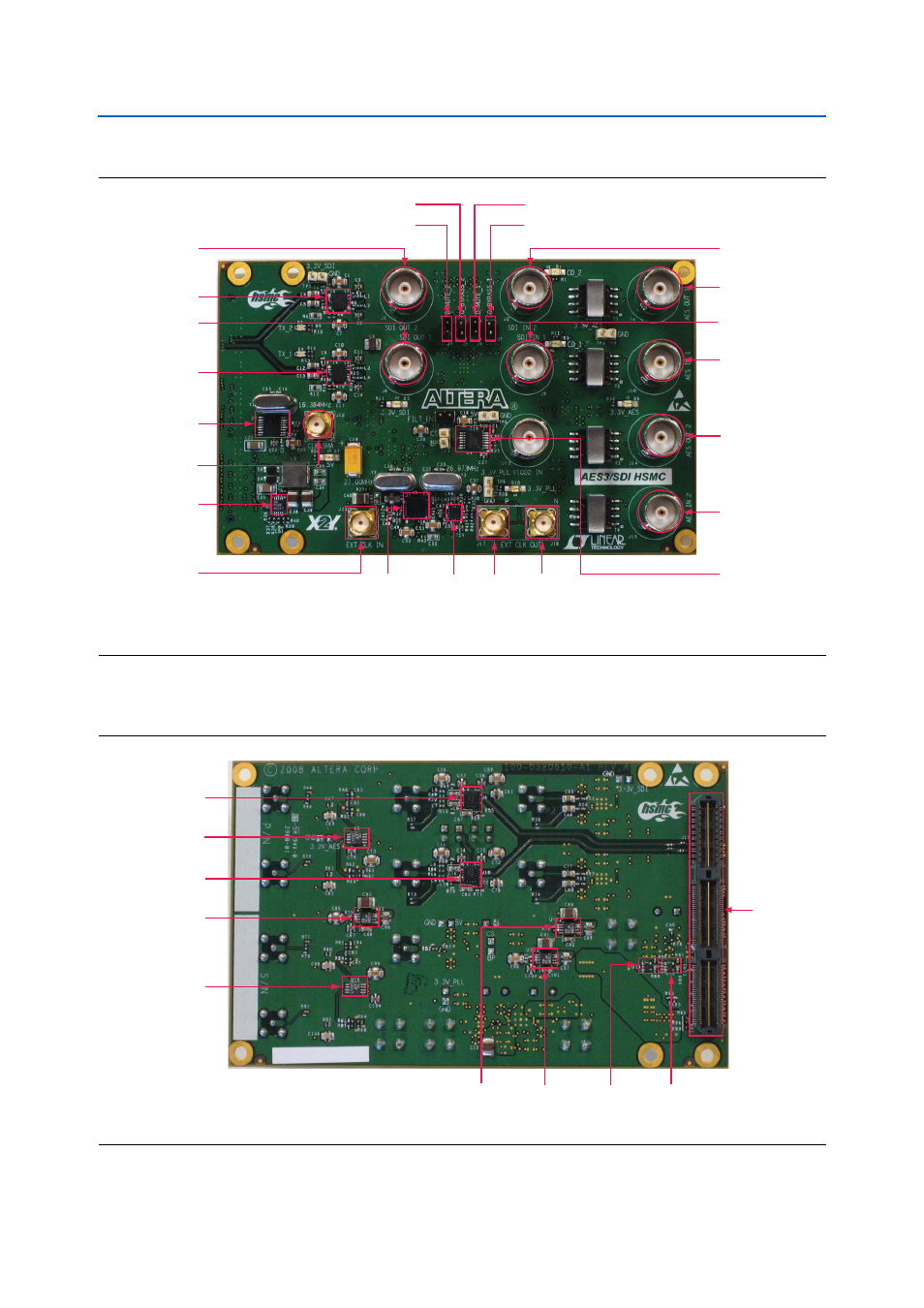
Figure 2–1. Top View of the SDI HSMC
SMA SDI
Clock Input (J16)
LVPECL
Differential
Clock
Buffer
(J62)
Equalizer Bypass Jumper (J7)
High Frequency
Switching
Regulator (U5)
AES VCXO PLL (U3)
SDI Input
Channel 2 (J2)
Multi-format Video
Sync Separator (U4)
SMA SDI
Clock
Output
(P)
(J17)
SDI
Multi-frequency
VCXO
Femto Clock
Video PLL (U6)
SDI Cable
Tri-speed Driver (U1)
AES Output
Channel 1 (J3)
AES Input
Channel 1 (J10)
AES Output
Channel 2 (J14)
AES Input
Channel 2 (J15)
SDI Output
Channel 2 (J1)
Carrier Detect — Mute Jumper (J4)
SDI Input
Channel 1 (J9)
Carrier Detect — Mute Jumper (J6)
Equalizer Bypass Jumper (J5)
SDI Output
Channel 1 (J8)
SDI Cable
Tri-speed Driver (U2)
SMA SDI
Clock
Output
(N)
(J18)
SMA AES
Clock Output (J12)
Figure 2–2. Bottom View of the SDI HSMC (HSMC Connector View)
Single Gate
Tri-state
Buffer (U14)
RS422 Transceiver (U9)
HSMC
Connector (J19)
Linear
Regulator
(U13)
Linear Regulator (U11)
SDI Cable
Equalizer (U8)
SDI Cable
Equalizer (U10)
Linear
Regulator
(U12)
RS422 Transceiver (U16)
Single Gate
Tri-state
Buffer (U15)