Aes3 clock, Aes3 clock –11 – Altera SDI HSMC User Manual
Page 19
Chapter 2: Board Components
2–11
Clock Circuitry
© July 2009 Altera Corporation
Loop Back Reference Clock From SDI Input
When an RX channel is locked onto the input data stream, the recovered clock
represents the actual bit rate of that stream. This recovered clock is often 74.25 MHz
and can be buffered from the host board and driven out through the HSMC interface
to the clock generator on the SDI HSMC. The clock output from the host is cleaned
(jitter), multiplied to 148.5 MHz, and driven back to the host board to be used as the
SERDES reference clock. Using this technique maintains the flow through timing.
Studio Reference Timing
If a studio clock source (a 27-MHz source) is available, the source can be connected to
the EXT CLK IN SMA port on the daughtercard.
Studio Reference Video Timing
A video synchronization separator is provided to synchronize the SDI video output
streams to analog video. The horizontal and vertical syncs are driven to the host board
and can be driven back to the video clock generator chip to produce a 148.5-MHz
SERDES reference.
shows the board's clock distribution.
AES3 Clock
AES3 clocking uses a semi-custom clock device from IDT (ICS275-22). The device
comes pre-programmed to produce 93.304 MHz, 90.3168 MHz (4× oversampling),
122.88 MHz, and 112.896 MHz (5× oversampling) from a 16.384-MHz crystal. Most
combinations are available at outputs CLK1 and CLK2. Output CLK1 is connected to
the HSMC connector and drives a signal to the host device. Output CLK2 is connected
to an output SMA connector. You can use this output for a reference, to trigger test
equipment, or to sync a signal to other devices in the AES3 system.
The base part (ICS275) is a VCXO that can have various combinations of input,
output, and feedback dividers to produce variations of the crystal frequency. The
control voltage input of the device is controlled by a passive network of resistors and
capacitors that are connected to tri-state buffers, one driven high and the other driven
low when in the active state (non-tri-stated). The single gate devices are powered by
3.3 V to allow full swing of the control voltage (V
IN
, AES_CLK_V) because the ICS275
is also powered by 3.3 V. The tri-state-enabled pins are controlled by the host device
connected to the HSMC. These pins should not be allowed to float.
To use the ICS275 as a normal oscillator and not as a VCXO, drive signals
AES_VCXO_UP
and AES_VCXO_DN both to logic 1. Both output signals are enabled
and the resulting voltage output after the resistor or capacitor network is a
mid-voltage driven to the V
IN
of the ICS275 device.
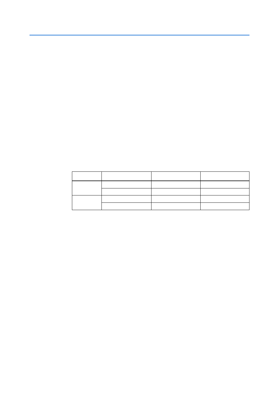
Table 2–8. SDI HSMC Clock Distribution
Frequency
Schematic Signal Name
Signal Originates From
Signal Propagates To
148.5 MHz
SDI_CLK_P
U7.12
J19.156 (HSMC)
SDI_CLK_N
U7.11
J19.168 (HSMC)
98.304 MHz
AES_CLK,
U3.5
J19.96 (HSMC)
AES_CLK_SMA
U3.6
J12 (SMA)