Aes3 rx channels, Aes3 tx channels, Aes3 rx channels –17 aes3 tx channels –17 – Altera SDI HSMC User Manual
Page 25
Chapter 2: Board Components
2–17
Audio/Video Input and Output
© July 2009 Altera Corporation
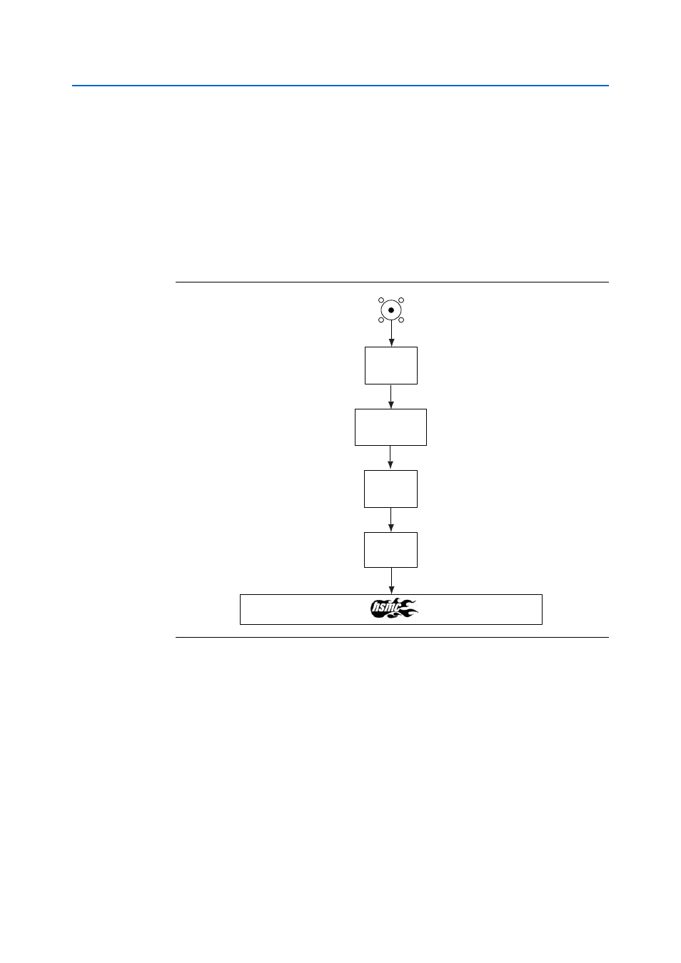
AES3 RX Channels
The AES3 RX channel delivers a 75-
Ω load termination with a return loss of 25 dB or
more.
shows a simplified block diagram of the AES3 RX channel. The
signal is input through a 75-
Ω BNC and terminated with a 75-Ω resistor to ground.
The unbalanced signal is then balanced through an isolation transformer. The
differential signal output from the transformer is biased and input to a RS422
transceiver. The output of the RS422 transceiver is a single-ended LVCMOS signal
which is driven to the host board through the HSMC connector.
shows the AES3 RX channel block diagram.
AES3 TX Channels
The AES3 TX channel is designed to have a balanced signal driver to the isolation
transformer. The output of the RS422 transceiver has an RX network to limit the
output slew rate, thus limiting the bandwidth of AES3 output. The AES3 channel is
designed to support 192-kHz to 24-kHz sample rates. The output is unbalanced with a
source impedance of 75
Ω and a return loss of 25 dB or more. The peak-to-peak output
voltage is 1.0 V centered around the ground of the transmitter.
shows the AES3 TX channel block diagram.
Figure 2–9. AES3 RX Channel Block Diagram
AES3 RX
Bias
Resistor
Resistor
Termination
Isolation
Transformer
RS422
Driver