Development board block diagram, Development board block diagram –2, Sdi –2 – Altera SDI HSMC User Manual
Page 6
1–2
Chapter 1: Overview
Board Component Blocks
© July 2009 Altera Corporation
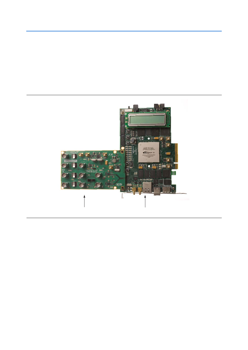
shows the SDI HSMC connected to an Altera FPGA development board.
f
for an
example of connecting the SDI HSMC to a host board.
f
For detailed information about the board components and interfaces of the Stratix IV
GX FPGA development board, refer to the
.
Development Board Block Diagram
shows the functional block diagram of the SDI HSMC. The board has three
distinct areas of interest:
■
SDI
■
AES
■
Clocking
SDI
The SDI includes two high-speed output interfaces from the HSMC to the cable
drivers and to two single-ended 75-
Ω BNC output interfaces. There are also two
receive paths which input signals to two 75-
Ω BNC connectors to receive equalizers.
The differential signals are then output to the HSMC connector.
Figure 1–1. SDI HSMC Connected to the Stratix IV GX FPGA Development Board
SDI HSMC
Stratix IV GX FPGA Development Board