Altera SDI HSMC User Manual
Page 31
Chapter 2: Board Components
2–23
Components and Interfaces
© July 2009 Altera Corporation
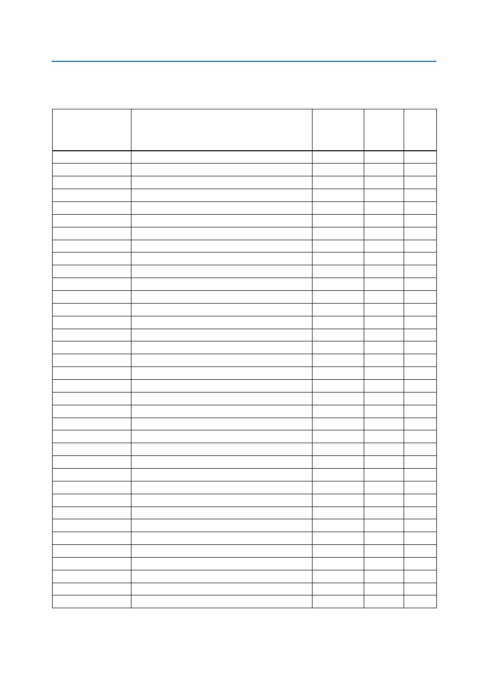
lists the HSMC connector schematic signal names and functions.
Table 2–13. HSMC Connector Schematic Signal Names And Functions (Part 1 of 2)
Schematic Signal
Name
Description
Direction
(with respect
to the SDI
HSMC)
HSMC Pin
Type
SDI_TX_P1
Differential transmitted data input to the cable driver
Input
29
CML
SDI_TX_N1
Differential transmitted data input to the cable driver
Input
31
CML
SDI_TX_P2
Differential transmitted data input to the cable driver
Input
25
CML
SDI_TX_N2
Differential transmitted data input to the cable driver
Input
27
CML
SDI_EQOUT_P1
Differential received data output from the cable equalizer
Output
30
CML
SDI_EQOUT_N1
Differential received data output from the cable equalizer
Output
32
CML
SDI_EQOUT_P2
Differential received data output from the cable equalizer
Output
26
CML
SDI_EQOUT_N2
Differential received data output from the cable equalizer
Output
28
CML
JTAG_TDO_TDI
JTAG data loop through
Input/Output
37, 38
CMOS
SDI_LED_TX_R1
Red LED signal for transmit channel 1
Input
41
CMOS
SDI_LED_TX_R2
Red LED signal for transmit channel 2
Input
43
CMOS
SDI_LED_TX_G1
Green LED signal for transmit channel 1
Input
47
CMOS
SDI_LED_TX_G2
Green LED signal for transmit channel 2
Input
49
CMOS
SDI_LED_RX_R1
Red LED signal for receive channel 1
Input
59
CMOS
SDI_LED_RX_R2
Red LED signal for receive channel 2
Input
53
CMOS
SDI_LED_RX_G1
Green LED signal for receive channel 1
Input
61
CMOS
SDI_LED_RX_G2
Green LED signal for receive channel 2
Input
55
CMOS
SDI_RATE_SEL1
Cable driver’s slew rate select for desired bit rate
Input
71
CMOS
SDI_RATE_SEL2
Cable driver’s slew rate select for desired bit rate
Input
73
CMOS
EQ_BYPASS1
Equalizer bypass for receive channel 1
Input
77
CMOS
EQ_BYPASS2
Equalizer bypass for receive channel 2
Input
79
CMOS
AES_CLK_SEL0
AES frequency select
Input
83
CMOS
AES_CLK_SEL1
AES frequency select
Input
85
CMOS
AES_CLK_SEL2
AES frequency select
Input
89
CMOS
AES_CLK_PDTSn
AES clock power down and tri-state
Input
91
CMOS
AES_OUT1
AES data output 1
Input
101
CMOS
AES_OUT2
AES data output 2
Input
103
CMOS
AES_VCXO_UP
AES VCXO frequency control
Input
107
CMOS
AES_VCXO_DN
AES VCXO frequency control
Input
109
CMOS
SDI_CLK_SEL
SDI clock input select
Input
113
CMOS
SDI_XTAL_SEL
SDI clock crystal select
Input
115
CMOS
SDI_CLK_BP0
SDI clock control
Input
119
CMOS
SDI_CLK_BP1
SDI clock control
Input
121
CMOS
SDI_CLK_N0
SDI clock control
Input
127
CMOS
SDI_CLK_N1
SDI clock control
Input
131
CMOS
SDI_CLK_V0
SDI clock control
Input
133
CMOS