Aes –3 clocking –3 – Altera SDI HSMC User Manual
Page 7
Chapter 1: Overview
1–3
Board Component Blocks
© July 2009 Altera Corporation
AES
The AES includes two input and two output interfaces. The interface to the host board
is 2.5-V CMOS signaling. The differential RS 422 line transceivers convert the
single-ended signal to balanced differential outputs which drive the audio isolation
transformers.
Clocking
Clocking is the third area of interest on the board. Clocking for the SDI interfaces is
supported by a dual SDI multi-frequency VCXO femto clock video PLL
(ICS810001-21) from Integrated Device Technology (IDT). The chipset supports
various inputs related to common video signals from the bit rate clocks or horizontal
sync signals. The output of the chipset is fed into a differential clock buffer. The
differential signal is then output to the HSMC connector and SMA connectors. Two
crystal oscillators are used in this chipset — 27 MHz and 27/1.001 MHz (26.973 MHz).
The PLL is used to supply 74.25 MHz or 148.5 MHz reference clocks to the transceiver
on the host board.
Clocking for the AES interfaces is implemented by using the VCXO PLL (ICS275-22),
a pre-programmed IDT part. As applied in the AES interface, a 16.384-MHz crystal is
used in the VCXO section and followed by a PLL to produce the supported
frequencies of 98.304 MHz, 90.3168 MHz, 122.88 MHz, and 112.896 MHz.
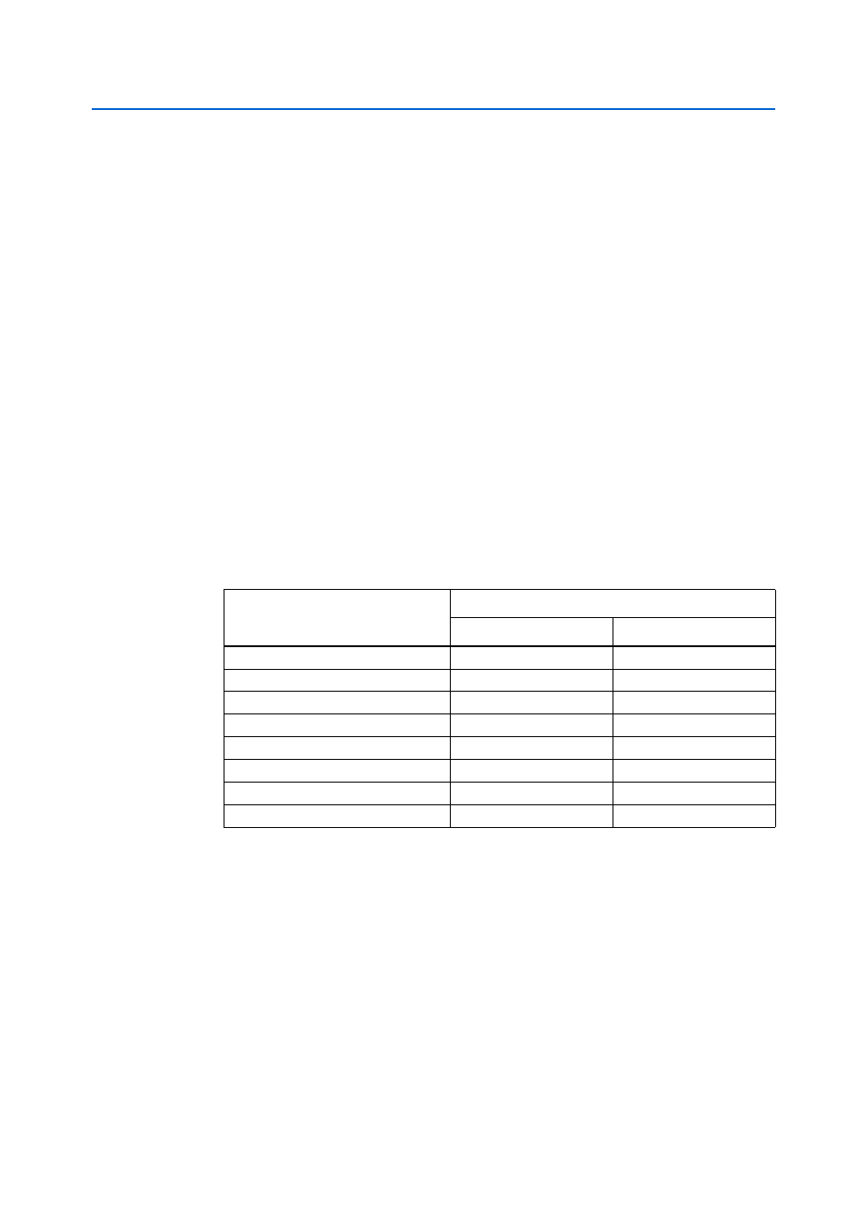
shows the frequency setup of the VCXO PLL.
Table 1–1. Frequency Setup of the VCXO PLL
S [2:0]
Frequency (MHz)
Pin 5
Pin 6
000
98.304
98.304
001
90.3168
90.3168
010
122.88
122.88
011
112.896
112.896
100
98.304
122.88
101
90.3168
112.896
110
98.304
90.3168
111
122.88
112.896