Altera SDI HSMC User Manual
Page 20
2–12
Chapter 2: Board Components
Clock Circuitry
© July 2009 Altera Corporation
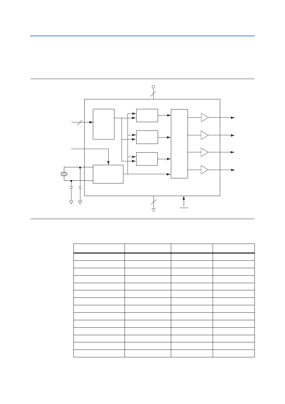
To use the ICS275 as a VCXO in a PLL application, connect the phase detector to the
AES3 up and down control signals.
shows the AES VCXO PLL block diagram.
shows the audio rate and clock frequencies supported by the SDI HSMC.
Figure 2–6. AES VCXO PLL Block Diagram
16.384 MHz
Crystal Input
Voltage-controlled
Crystal Oscillator
2
3
PLL1
PLL2
PLL3
One-time-
programmable
ROM
with PLL
Values
Divide
Logic
and
Output
Enable
Control
CLK1
CLK2
CLK3
CLK4
PDTS
GND
External Capacitors
S2:S0
VDD
X1
X2
V
IN
3
Table 2–9. Audio Sample Rate versus Clock Frequency (Part 1 of 2)
Audio Sample Rate (kHz)
Bit Rate Clock (MHz)
Oversampling Rate
VCXO Frequency
24.00
3.0720
32
98.3040
32.00
4.0960
24
98.3040
44.10
5.6448
16
90.3168
48.00
6.1440
16
98.3040
88.20
11.2896
8
90.3168
96.00
12.2880
8
98.3040
176.4
22.5792
4
90.3168
192
24.5760
4
98.3040
24.00
3.0720
40
122.8800
32.00
4.0960
30
122.8800
44.10
5.6448
20
112.8960
48.00
6.1440
20
122.8800
88.20
11.2896
10
112.8960
96.00
12.2880
10
122.8800