Component summary, Component summary –6, Fpga – Altera Cyclone II FPGA Starter Development Board User Manual
Page 14
1–6
Reference Manual
Altera Corporation
Cyclone II FPGA Starter Development Board
October 2006
Introduction
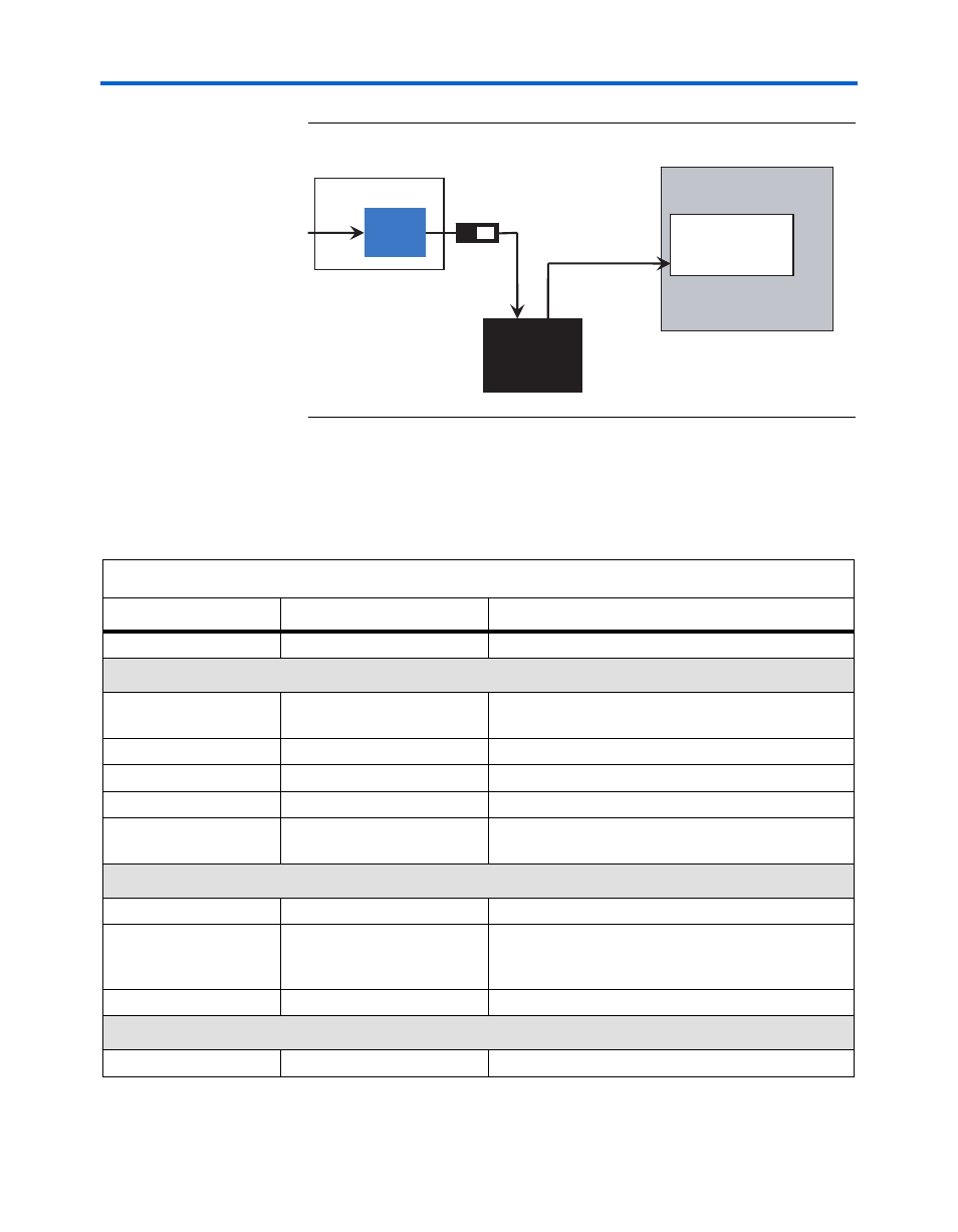
Figure 1–4. AS Configuration Setup
Component
Summary
lists the components, their locations, and brief descriptions.
USB Blaster Circuit
MAX
3128
USB
FPGA
JTAG Config Port
EPCS Serial
Configuration
Device
RUN/PROG
PROG”
Auto Power on Config
Table 1–1. Cyclone II FPGA Development Board Components & Interfaces (Part 1 of 2)
Board Designation
Name
Description
U2
Cyclone II FPGA
EP2C20 device
User Interface
KEY0 – KEY3
Push-button switches
Four momentary contact switches for user input to the
FPGA
SW0 – SW9
Toggle switches
Ten toggle switches for configuration of the FPGA
LEDG0 – LEDG7
Individual LEDs
Eight green LEDs driven by the FPGA
LEDR0 – LEDR9
Individual LEDs
Ten red LEDs driven by the FPGA
HEX0 – HEX3
Seven-segment LEDs
Four seven-segment LEDs that display numeric
output from the FPGA
Memory
U7
SRAM memory
512 KBytes of SRAM
U9
Flash memory
4 MBytes of nonvolatile memory for use by both the
FPGA and the configuration controller. LED7 lights
whenever the flash chip-enable asserts.
U6
DDR SDRAM memory
8 MBytes of DDR SDRAM.
Connections & Interfaces
PS2KB
PS/2 connector
PS/2 keyboard connector