Vga circuit pin list, Vga circuit schematic – Altera Cyclone II FPGA Starter Development Board User Manual
Page 22
2–4
Reference Manual
Altera Corporation
Cyclone II FPGA Starter Development Board
October 2006
Development Board Components
lists the VGA vertical timing specifications.
VGA Circuit Pin List
lists the FPGA pins assigned to the VGA circuit.
VGA Circuit Schematic
shows the VGA circuit schematic.
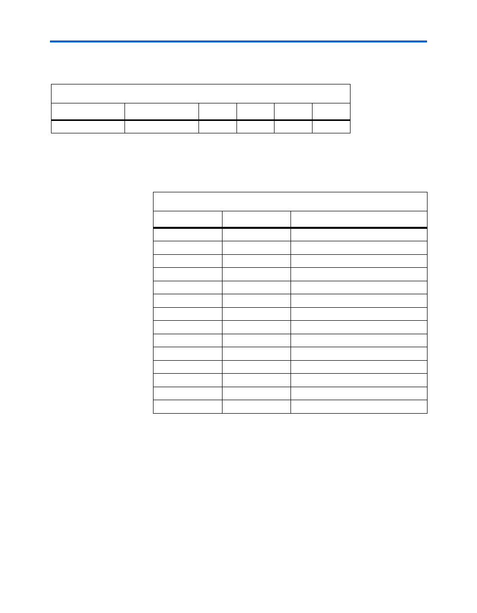
Table 2–3. VGA Vertical Timing Specifications
Configuration
Resolution (HxV)
a (lines)
b (lines)
c (lines)
d (lines)
VGA (60 Hz)
640 x 480
2
33
480
10
Table 2–4. VGA Circuit FPGA Pin Connections
Signal Name
FPGA Pin
Description
VGA_R[0]
PIN_D9
VGA Red[0]
VGA_R[1]
PIN_C9
VGA Red[1]
VGA_R[2]
PIN_A7
VGA Red[2]
VGA_R[3]
PIN_B7
VGA Red[3]
VGA_G[0]
PIN_B8
VGA Green[0]
VGA_G[1]
PIN_C10
VGA Green[1]
VGA_G[2]
PIN_B9
VGA Green[2]
VGA_G[3]
PIN_A8
VGA Green[3]
VGA_B[0]
PIN_A9
VGA Blue[0]
VGA_B[1]
PIN_D11
VGA Blue[1]
VGA_B[2]
PIN_A10
VGA Blue[2]
VGA_B[3]
PIN_B10
VGA Blue[3]
VGA_HS
PIN_A11
VGA H_SYNC
VGA_VS
PIN_B11
VGA V_SYNC