Push button switch schematic, Push button switch pin list, Toggle switches – Altera Cyclone II FPGA Starter Development Board User Manual
Page 35
Altera Corporation
Reference Manual
2–17
October 2006
Cyclone II FPGA Starter Development Board
Development Board Components
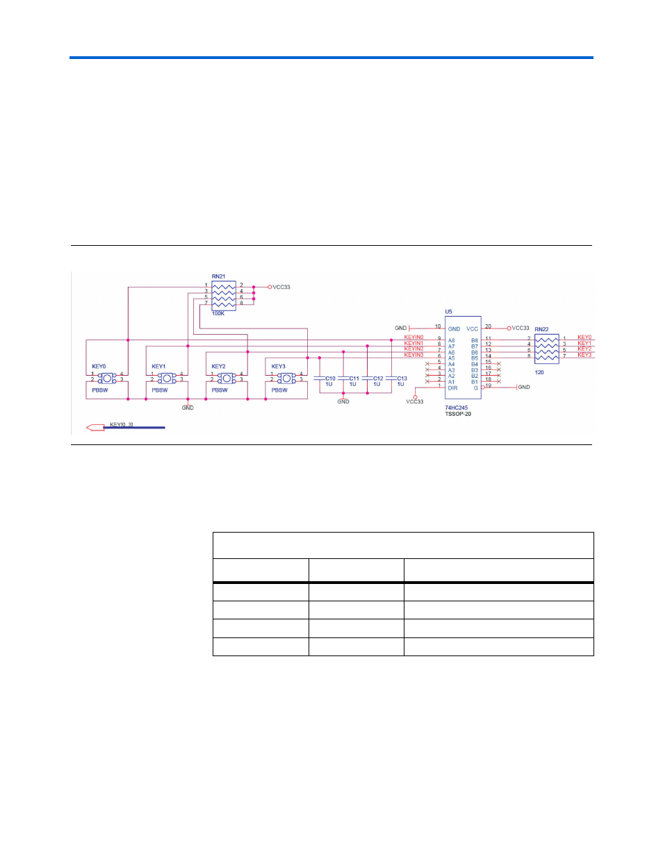
The switches connect to an FPGA general-purpose I/O pin with a pull-up
resistor through the Schmitt Trigger outputs, KEY0, …, KEY3. Each I/O
pin senses a logic level 0 when the corresponding switch is pressed.
The debounced outputs enable users to use the push buttons as clock or
reset inputs for a circuit.
Push Button Switch Schematic
shows a schematic diagram of the push button switches.
Figure 2–12. Push Button Switch Schematic Diagram
Push Button Switch Pin List
lists the FPGA pins assigned to the push button switches.
Toggle Switches
The development board provides ten sliding
toggle switches,
SW0
–SW9, located at the bottom left on the development board below
the red LEDs, LEDR0-LEDR9 (
). Not debounced, these
switches provide level-sensitive data inputs to a circuit. Each switch
Table 2–10. Push Button Switch FPGA Pin Connections
Switch
FPGA Pin
Description
KEY[0]
PIN_R22
Pushbutton[0]
KEY[1]
PIN_R21
Pushbutton[1]
KEY[2]
PIN_T22
Pushbutton[2]
KEY[3]
PIN_T21
Pushbutton[3]