Vga timing – Altera Cyclone II FPGA Starter Development Board User Manual
Page 21
Altera Corporation
Reference Manual
2–3
October 2006
Cyclone II FPGA Starter Development Board
Development Board Components
The FPGA provides the synchronization signals directly to the VGA port,
a16-pin D-SUB connector, VGA, located at the top edge of the board,
while the DAC, using a resistor network, produces the red, green, and
blue (RGB) analog data signals.
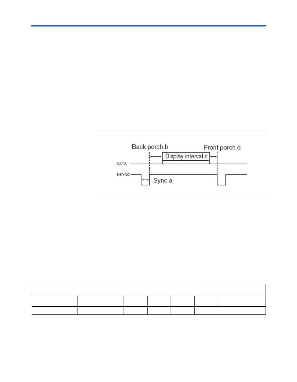
VGA Timing
illustrates the basic timing requirements for each horizontal
line, or row, displayed on a VGA monitor. An active-LOW pulse of time
duration a (
) applied to the horizontal synchronization input,
hsync
, of the monitor marks the end of one row of data and the start of
the next. After the hsync pulse, the RGB data inputs on the monitor must
be off, driven to 0 volts, for a backporch time period b.
Figure 2–1. VGA Horizontal Timing
The display interval starts after the backporch time period b expires. For
a time duration c, the RGB data inputs turn on and RGB data drives each
pixel in turn across the row. After the display completes, the RGB data
inputs must again turn off for a frontporch period d before the next hsync
pulse restarts the process on the next row.
The vertical synchronization timing resembles the diagram in
,
except a vsync pulse marks the end of one frame and the start of the next,
and the data display refers to the set of rows in the frame.
lists the VGA horizontal timing specifications.
Table 2–2. VGA Horizontal Timing Specifications
Configuration
Resolution (HxV)
a (
μs)
b (
μs)
c (
μs)
d (
μs)
Pixel clock (MHz)
VGA (60 Hz)
640 x 480
3.8
1.9
25.4
0.6
25 (640/c)