Table 8-70, Spp boot bank selection, Cpld and fpga – Artesyn ATCA-8310 Installation and Use (May 2014) User Manual
Page 298: 6 spp boot bank selection
Advertising
CPLD and FPGA
ATCA-8310 Installation and Use (6806800M72E)
298
8.2.2.3.6 SPP Boot Bank Selection
15:8
Inverted level of Switch Signals SW_[7:0]
Bit 0: SW5 Pin 1
Bit 1: SW5 Pin 2
Bit 2: SW5 Pin 3
Bit 3: SW5 Pin 4
Bit 4: SW6 Pin 1
Bit 5: SW6 Pin 2
Bit 6: SW6 Pin 3
Bit 7: SW6 Pin 4
Note: The default values may be overwritten by SPP write access.
Ext.
SW_[7:0]
SPP: r/w
Table 8-69 Status Register (continued)
Address: 0x06 - 0x07
Bit Description
Default
Access
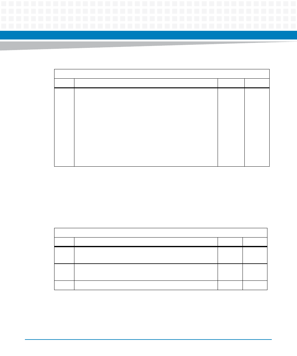
Table 8-70 SPP Boot Bank Selection
Address: 0x08
Bit Description
Default
Access
0
SPP Current Selected Bank.
Latched signal SPP_FLASH_SEL with rising edge of SPP_HRESET_
Ext.
r
1
SPP Selected Bank.
Level of signal SPP_FLASH_SEL
Ext.
r
7:2
Reserved
0
r
Advertising
This manual is related to the following products: