Jtag chain header, Jtag chain header –19 – Altera Arria II GX FPGA Development Board User Manual
Page 27
Chapter 2: Board Components
2–19
Configuration, Status, and Setup Elements
February 2011
Altera Corporation
Arria II GX FPGA Development Board Reference Manual
lists the board settings DIP switch component reference and
manufacturing information.
JTAG Chain Header
The JTAG chain header (J9) either remove or include devices in the active JTAG chain
by removing or installing the jumper shunts. However, the Arria II GX FPGA device
is always in the JTAG chain.
shows the header controls and its
descriptions.
lists the JTAG chain header component reference and manufacturing
information.
7
CLK_ENABLE
ON : On-board oscillators enable
OFF : On-board oscillators disable
ON
8
CLK_SEL
ON : 100 MHz clock select
OFF : SMA input clock select
ON
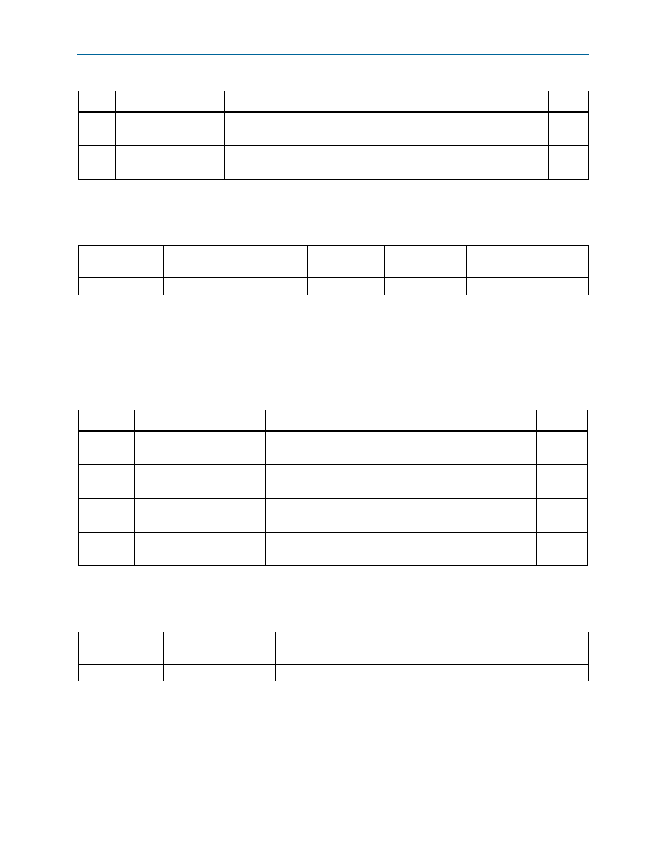
Table 2–13. Board Settings DIP Switch Controls (Part 2 of 2)
Switch Schematic Signal Name
Description
Default
Table 2–14. Board Settings DIP Switch Component Reference and Manufacturing Information
Board Reference
Description
Manufacturer
Manufacturer
Part Number
Manufacturer Website
SW4
Eight-Position slide DIP switch
HCH
HPS608-E
Table 2–15. JTAG Chain Header Controls
Switch
Schematic Signal Name
Description
Default
1
MAX_JTAG_EN
ON : Bypass MAX II CPLD EPM2210 System Controller
OFF : MAX II CPLD EPM2210 System Controller in-chain
OFF
2
HSMA_JTAG_EN
ON : Bypass HSMA
OFF : HSMA in-chain
ON
3
HSMB_JTAG_EN
ON : Bypass HSMB
OFF : HSMB in-chain
ON
4
PCIE_JTAG_EN
ON : Bypass PCI Express
OFF : Reserved (disables JTAG chain, do not use)
ON
Table 2–16. JTAG Chain Header Component Reference and Manufacturing Information
Board Reference
Device Description
Manufacturer
Manufacturer
Part Number
Manufacturer Website
J9
2x4 100 mil jumper
Leamax Enterprise Co.
21312*4SE