Clock circuitry, Arria ii gx fpga clock inputs, Clock circuitry –21 – Altera Arria II GX FPGA Development Board User Manual
Page 29: Arria ii gx fpga clock inputs –21, Pll 5 pll 6
Chapter 2: Board Components
2–21
Clock Circuitry
February 2011
Altera Corporation
Arria II GX FPGA Development Board Reference Manual
Clock Circuitry
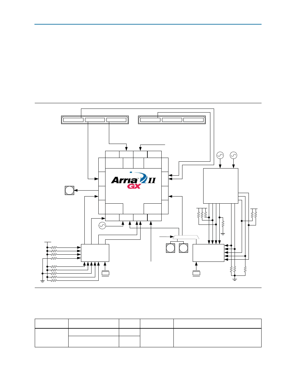
This section describes the board's clock inputs and outputs.
Arria II GX FPGA Clock Inputs
The development board has two types of clock inputs—global clock inputs and
transceiver reference clock inputs.
shows the Arria II GX FPGA development board clock inputs.
shows the external clock inputs for the Arria II GX FPGA development
board.
Figure 2–6. Arria II GX FPGA Development Board Clock Inputs
Q 0
Q 1
Q 2
Q 3
3B
3A
4A
4B
8B
8A
7A
7B
6 B
6 A
5 A
5 B
PLL 1
PLL 2
PLL 3
PLL 4
EP2AGX125EF35
Control signals route
to MAX II
155.52 M
CLK_SEL
REFCLK INPUT
SMA
SMA
(LVPECL)
2-to-4 buffer
MAX II CPLD
EPM2210 System Controller
25 MHz
Crystal
3 .3 V
Low Jitter Clock
Generator*
(Default 125 MHz)
CDCM61004RHB
XIN 2
(LVDS)
CL
K
1
_
R
S
T
n
CL
K
1
_
C
E
C
LK
1
_
OS
1
CL
K
1
_
O
S
0
CL
K1
_
P
R1
CL
K1
_
P
R0
CL
K1
_
O
D2
CL
K1
_
O
D1
CL
K1
_
O
D0
3 .3 V
(LVPECL)
CLK 2 _ RSTn
CLK 2 _ CE
CLK 2 _ OS 1
CLK 2 _ OS 0
CLK 2 _ PR 1
CLK 2 _ PR 0
CLK 2 _ OD 2
CLK 2 _ OD 1
CLK 2 _ OD 0
3 .3 V
PC
IE
_
R
E
F
C
L
K_
P/
N
XIN 1
7 6 5 4 3 2 1 0
7 6 5 4 3 2 1 0
HS
M
A
_
C
L
K
_
IN_
P
[1
]/
N
[1
]
(L
V
D
S
)
HSMA CLK_IN_P[2]/N[2]
(LVDS)
HSMB_CLK_IN0
HSMA_CLK_IN0
* CDCM6100x can be set to output frequencies
of 100 MHz, 125 MHz, 156.25 MHz.
PLL
5
PLL
6
25 MHz
Crystal
CL
K
_
IN
_
T
O
P
_
P
/N
CL
K
_
IN
_
B
O
T
_
P
/N
CLOCK_SMA
SMA
100 M
50 M
ENET_RX_CLK
(2.5 V)
Low Jitter Clock
Generator*
(Default 100 MHz)
CDCM61001RHB
(2.5 V)
(2.5 V)
(LVDS)
(LVDS)
(LVDS)
(L
V
D
S
)
(L
V
D
S
)
Table 2–20. Arria II GX FPGA Development Board Clock Inputs (Part 1 of 2)
Source
Schematic Signal Name
Pin
I/O Standard
Description
U25
CLK_155_P
R29
LVPECL
155.52 MHz oscillator which drives the
transceiver Q2 reference clock input with
100
OCT.
CLK_155_N
R30