Altera Arria II GX FPGA Development Board User Manual
Page 50
2–42
Chapter 2: Board Components
Memory
Arria II GX FPGA Development Board Reference Manual
February 2011
Altera Corporation
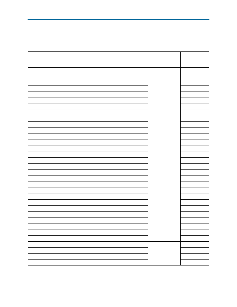
lists the DDR2 SODIMM pin assignments, signal names, and its functions.
The signal names and types are relative to the Arria II device in terms of I/O setting
and direction.
Table 2–42. DDR2 SODIMM Pin Assignments, Signal Names and Functions (Part 1 of 4)
Board Reference
Description
Schematic Signal
Name
I/O Standard
Arria II GX
Device
Pin Number
J7.102
Address bus
DDR2_A0
1.8-V SSTL Class I
AH14
J7.101
Address bus
DDR2_A1
AK12
J7.100
Address bus
DDR2_A2
AE12
J7.99
Address bus
DDR2_A3
AH13
J7.98
Address bus
DDR2_A4
AF14
J7.97
Address bus
DDR2_A5
AG12
J7.94
Address bus
DDR2_A6
AJ18
J7.92
Address bus
DDR2_A7
AL19
J7.93
Address bus
DDR2_A8
AG13
J7.91
Address bus
DDR2_A9
AE13
J7.105
Address bus
DDR2_A10
AK10
J7.90
Address bus
DDR2_A11
AH23
J7.89
Address bus
DDR2_A12
AF13
J7.116
Address bus
DDR2_A13
AM5
J7.86
Address bus
DDR2_A14
AH24
J7.84
Address bus
DDR2_A15
AP28
J7.107
Bank address bus
DDR2_BA0
AJ11
J7.106
Bank address bus
DDR2_BA1
AJ13
J7.85
Bank address bus
DDR2_BA2
AE14
J7.113
Column address select
DDR2_CAS_n
AL8
J7.79
Clock enable
DDR2_CKE0
AP8
J7.110
Chip select rank 0
DDR2_CS_n0
AM13
J7.115
Chip select rank 1
DDR2_CS_n1
AL9
J7.114
Termination enable rank 0
DDR2_ODT0
AJ10
J7.119
Termination enable rank 1
DDR2_ODT1
AF12
J7.108
Row address select
DDR2_RAS_n
AH12
J7.197
EEPROM serial clock
DDR2_SCL
—
J7.195
EEPROM serial data
DDR2_SDA
—
J7.109
Write enable
DDR2_WE_n
AM6
J7.30
Clock P0
DDR2_CLK_P0
Differential 1.8-V
SSTL Class I
AJ7
J7.32
Clock N0
DDR2_CLK_N0
AK7
J7.164
Clock P1
DDR2_CLK_P1
AK6
J7.166
Clock N1
DDR2_CLK_N1
AL6