Power supply, Power supply –49 – Altera Arria II GX FPGA Development Board User Manual
Page 57
Chapter 2: Board Components
2–49
Power Supply
February 2011
Altera Corporation
Arria II GX FPGA Development Board Reference Manual
lists the flash component reference and manufacturing information.
Power Supply
A laptop-style DC power input supplies power to the development board. The input
voltage must be in the range of 14 V to 20 V. The DC voltage is then stepped down to
various power rails used by the components on the board and installed into the
HSMC connectors.
An on-board multi-channel analog-to-digital converter (ADC) measures both the
voltage and current for several specific board rails. A GUI displays the power
utilization by showing a graph of the power consumption versus time.
U23.E2
Data bus
FSM_D1
2.5-V
C18
U23.G3
Data bus
FSM_D2
D28
U23.E4
Data bus
FSM_D3
B19
U23.E5
Data bus
FSM_D4
E19
U23.G5
Data bus
FSM_D5
E18
U23.G6
Data bus
FSM_D6
G19
U23.H7
Data bus
FSM_D7
F19
U23.E1
Data bus
FSM_D8
D21
U23.E3
Data bus
FSM_D9
D23
U23.F3
Data bus
FSM_D10
D24
U23.F4
Data bus
FSM_D11
A25
U23.F5
Data bus
FSM_D12
B25
U23.H5
Data bus
FSM_D13
A26
U23.G7
Data bus
FSM_D14
C26
U23.E7
Data bus
FSM_D15
A27
U23.F6
Address valid
FLASH_ADVn
T4
U23.B4
Chip enable
FLASH_CEn
M3
U23.E6
Clock
FLASH_CLK
N4
U23.F8
Output enable
FLASH_OEn
K5
U23.F7
Ready
FLASH_RDYBSYn
R3
U23.D4
Reset
FLASH_RESETn
N3
U23.G8
Write enable
FLASH_WEn
C7
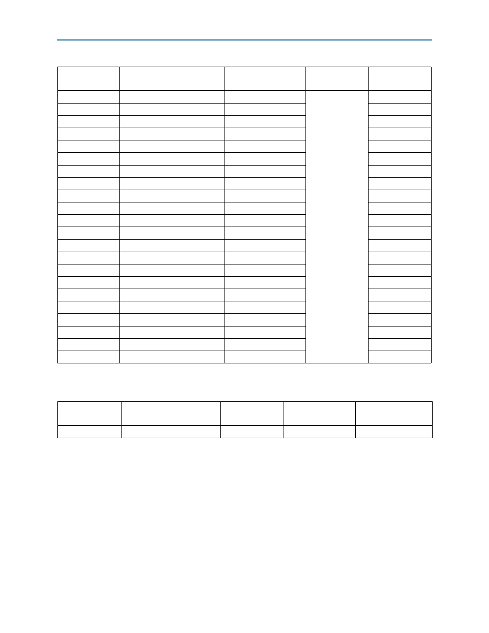
Table 2–46. Flash Pin Assignments, Schematic Signal Names, and Functions (Part 2 of 2)
Board Reference
Description
Schematic Signal Name
I/O Standard
Arria II GX Device
Pin Number
Table 2–47. Flash Component Reference and Manufacturing Information
Board Reference
Description
Manufacturer
Manufacturing
Part Number
Manufacturer
Website
U23
512-MB synchronous flash
Numonyx
PC28F512P30BF