Memory, Ddr3, Memory –39 – Altera Arria II GX FPGA Development Board User Manual
Page 47: Ddr3 –39
Chapter 2: Board Components
2–39
Memory
February 2011
Altera Corporation
Arria II GX FPGA Development Board Reference Manual
lists the HSMC connector component reference and manufacturing
information.
Memory
This section describes the board's memory interface support and also their signal
names, types, and connectivity relative to the Arria II GX device. The board has the
following memory interfaces:
■
DDR3
■
DDR2 SODIMM
■
SSRAM
■
Flash
f
For more information about the memory interfaces, refer to the following documents:
■
ection in volume 4 of the External Memory Interface Handbook.
■
on in volume 6 of the External Memory Interface
Handbook
DDR3
There is a single DDR3 device, providing 128-MB interface with a 16-bit data bus. This
memory interface runs at a maximum frequency of 400 MHz for a maximum
theoretical bandwidth of over 12.8 Gbps. The internal bus in the FPGA is typically 2 or
4 times the width at full-rate or half-rate respectively. For example, a 400 MHz 16-bit
interface becomes a 200 MHz 64-bit bus.
J1.158
Dedicated CMOS I/O bit 75
HSMB_D75
2.5-V
V5
J1.160
HSMC port B presence detect
HSMB_PSNT_n
AG28
D2
User LED to show RX data activity on
HSMC port B
HSMB_RX_LED
AF23
D3
User LED to show TX data activity on HSMC
port B
HSMB_TX_LED
AE24
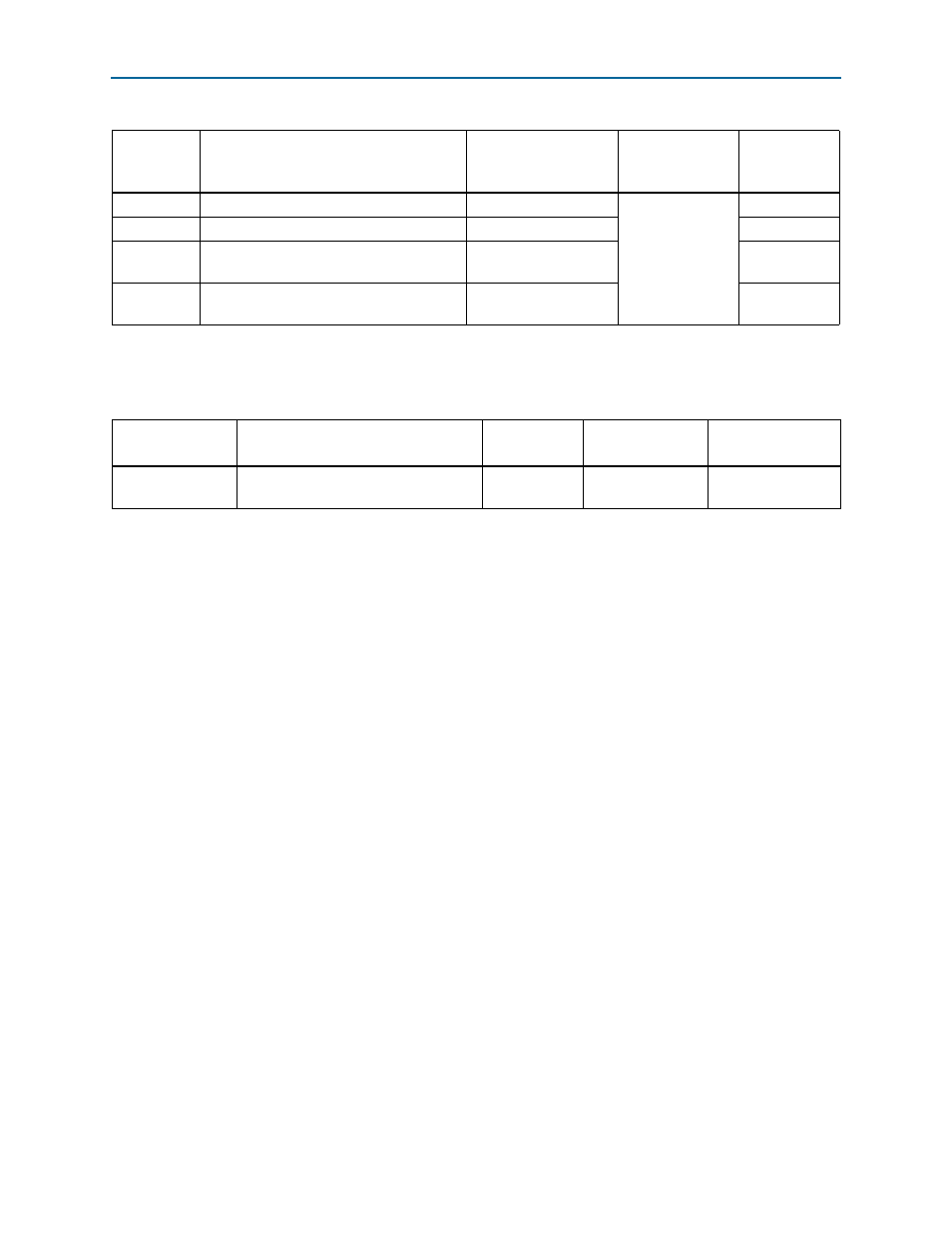
Table 2–38. HSMC Port B Pin Assignments, Schematic Signal Names, and Functions (Part 4 of 4)
Board
Reference
Description
Schematic Signal
Name
I/O Standard
Arria II GX
Device
Pin Number
Table 2–39. HSMC Connector Component Reference and Manufacturing Information
Board Reference
Description
Manufacturer
Manufacturing
Part Number
Manufacturer
Website
J1 and J2
HSMC, custom version of QSH-DP
family high-speed socket.
Samtec
ASP-122953-01