A. board revision history, Single-die flash version differences, Appendix a. board revision history – Altera Arria II GX FPGA Development Board User Manual
Page 61
February 2011
Altera Corporation
Arria II GX FPGA Development Board Reference Manual
A. Board Revision History
This appendix catalogs revisions to the Arria II GX FPGA development board.
lists the versions of all releases of the Arria II GX FPGA development
board.
Single-Die Flash Version Differences
The single-die flash version of the Arria II GX FPGA development board is created to
replace the obsolete dual-die flash device with a single-die flash device. The two flash
devices are equivalent except for some software routines used to access them because
the single-die device has only one CFI table whereas the duel-die device has two CFI
tables.
To determine which flash your board is using, refer to the device part number
installed at U23. The single-die package is smaller than the dual-die version.
f
For more information about the flash change and its application, refer to the
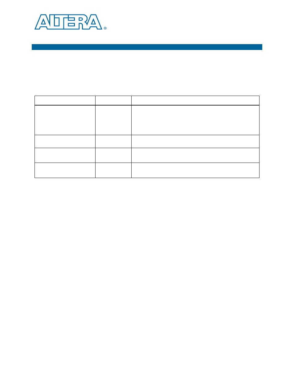
Table A–1. Arria II GX FPGA Development Board Revision History
Version
Release Date
Description
Production silicon
(Speed grade C4N device)
January 2011
Increased the maximum speeds of the following interfaces:
■
LVDS incresases to 1.25 Mbps from 1.05 Mbps.
■
DDR3 increases to 400 Mbps from 300 Mbps.
■
DDR2 increases to 333 Mbps from 300 Mbps.
Single-die flash
September 2010
Replaced Intel dual-die 512-Mb flash (PC48F4400P0VB00) with
Numonyx single-die flash (PC28F512P30BF).
Production silicon
(Speed grade C5N device)
July 2010
No board changes from engineering silicon version.
Engineering silicon
(Speed grade C5NES device)
September 2009
Initial release.