Altera Arria II GX FPGA Development Board User Manual
Page 48
2–40
Chapter 2: Board Components
Memory
Arria II GX FPGA Development Board Reference Manual
February 2011
Altera Corporation
lists the DDR3 pin assignments, signal names, and functions. The signal
names and types are relative to the Arria II device in terms of I/O setting and
direction.
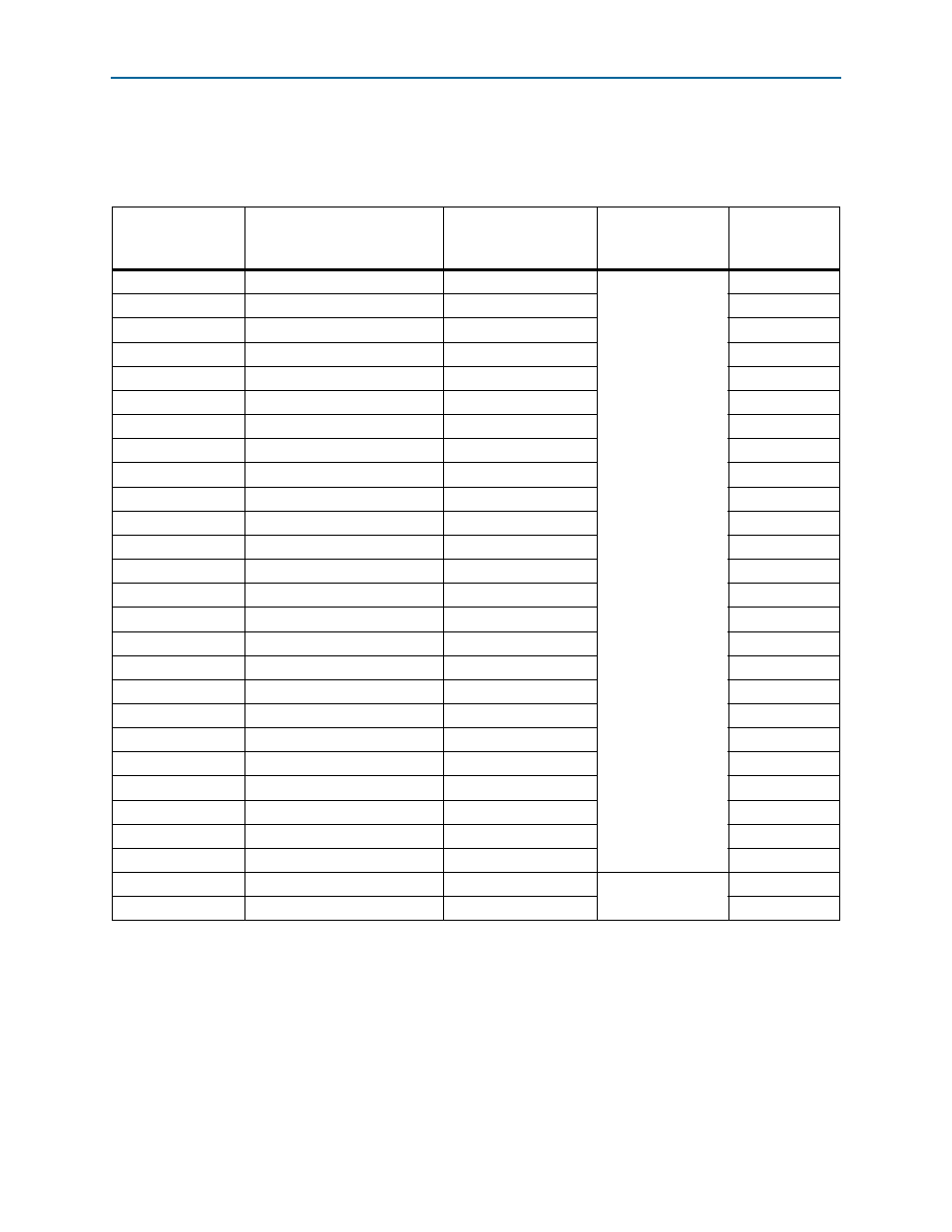
Table 2–40. DDR3 Pin Assignments, Schematic Signal Names, and Functions (Part 1 of 2)
Board Reference
Description
Schematic Signal
Name
I/O Standard
Arria II GX
Device
Pin Number
U13.N3
Address bus
DDR3_A0
1.5-V SSTL Class I
G16
U13.P7
Address bus
DDR3_A1
A12
U13.P3
Address bus
DDR3_A2
H18
U13.N2
Address bus
DDR3_A3
F16
U13.P8
Address bus
DDR3_A4
A7
U13.P2
Address bus
DDR3_A5
G17
U13.R8
Address bus
DDR3_A6
C13
U13.R2
Address bus
DDR3_A7
K14
U13.T8
Address bus
DDR3_A8
D11
U13.R3
Address bus
DDR3_A9
M16
U13.L7
Address bus
DDR3_A10
A11
U13.R7
Address bus
DDR3_A11
E15
U13.N7
Address bus
DDR3_A12
A8
U13.T3
Address bus
DDR3_A13
M17
U13.T7
Address bus
DDR3_A14
B15
U13.M2
Bank address bus
DDR3_BA0
D16
U13.N8
Bank address bus
DDR3_BA1
C12
U13.M3
Bank address bus
DDR3_BA2
C16
U13.K3
Column address select
DDR3_CAS_n
D15
U13.K9
Clock enable
DDR3_CKE
B10
U13.L2
Chip select
DDR3_CS_n
A10
U13.K1
Termination enable
DDR3_ODT
E16
U13.J3
Row address select
DDR3_RAS_n
A13
U13.T2
Reset
DDR3_RST_n
G18
U13.L3
Write enable
DDR3_WE_n
A15
U13.J7
Clock P
DDR3_CLK_P
Differential 1.5-V
SSTL Class I
B13
U13.K7
Clock N
DDR3_CLK_N
B12