Altera Arria II GX FPGA Development Board User Manual
Page 55
Chapter 2: Board Components
2–47
Memory
February 2011
Altera Corporation
Arria II GX FPGA Development Board Reference Manual
lists the SSRAM component reference and manufacturing information.
U22.F2
Data bus
FSM_D21
2.5-V
T10
U22.G1
Data bus
FSM_D22
P4
U22.G2
Data bus
FSM_D23
R11
U22.J1
Data bus
FSM_D24
A18
U22.J2
Data bus
FSM_D25
B18
U22.K1
Data bus
FSM_D26
C19
U22.K2
Data bus
FSM_D27
D19
U22.L1
Data bus
FSM_D28
B21
U22.L2
Data bus
FSM_D29
A21
U22.M1
Data bus
FSM_D30
C21
U22.M2
Data bus
FSM_D31
A22
U22.A8
Address status controller
SRAM_ADSCn
C10
U22.B9
Address status processor
SRAM_ADSPn
A20
U22.A9
Address valid
SRAM_ADVn
D9
U22.A7
Byte write enable
SRAM_WEn
J11
U22.B5
Byte lane 0 write enable
SRAM_BEN0
J13
U22.A5
Byte lane 1 write enable
SRAM_BEN1
H12
U22.A4
Byte lane 2 write enable
SRAM_BEN2
E9
U22.B4
Byte lane 3 write enable
SRAM_BEN3
H13
U22.A3
Chip enable
SRAM_CE1n
E10
U22.B6
Clock
SRAM_CLK
J12
U22.N11
Data bus parity byte lane 0
SRAM_DQP0
A24
U22.C11
Data bus parity byte lane 1
SRAM_DQP1
B22
U22.C1
Data bus parity byte lane 2
SRAM_DQP2
P9
U22.N1
Data bus parity byte lane 3
SRAM_DQP3
C22
U22.B7
Global write enable
SRAM_GWn
K12
U22.R1
Mode
SRAM_MODE
—
(Connects to the MAX II
CPLD EPM2210 System
Controller)
U22.B8
Output enable
SRAM_OEn
D10
U22.H11
Sleep
SRAM_ZZ
B27
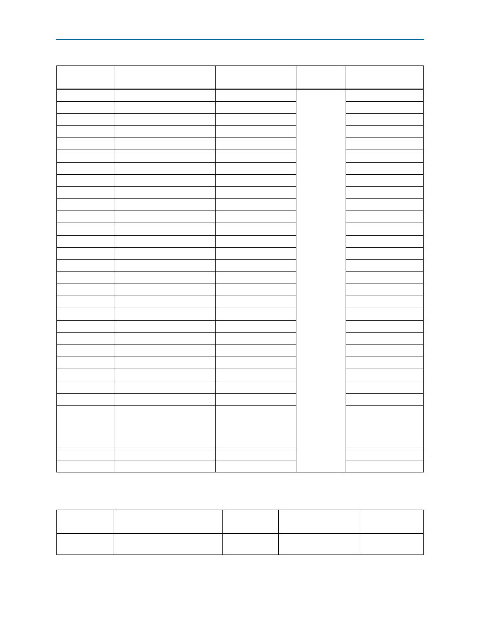
Table 2–44. SSRAM Pin Assignments, Schematic Signal Names, and Functions (Part 3 of 3)
Board Reference
Description
Schematic Signal Name
I/O Standard
Arria II GX Device
Pin Number
Table 2–45. SSRAM Component Reference and Manufacturing Information
Board Reference
Description
Manufacturer
Manufacturing
Part Number
Manufacturer
Website
U22
Standard synchronous pipelined
SCD, 512K × 36, 200 MHz
ISSI Inc.
IS61VPS51236A-200B3