Board components & interfaces, Board overview, Chapter 2. board components & interfaces – Altera Cyclone II EP2C35 PCI Development Board User Manual
Page 11: Board overview –1
Altera Corporation
Core Version 4.0.0
2–1
May 2005
Preliminary
2. Board Components &
Interfaces
Board Overview
This chapter provides operational and connectivity detail for the board’s
major components and interfaces.
f
For pin-outs and signal specifications, refer to
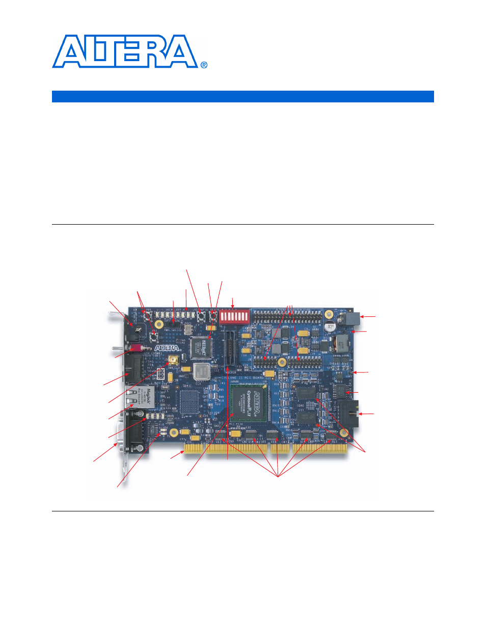
Figure 2–1
shows a top view of the Cyclone
™
II EP2C35 PCI Development
Board.
Figure 2–1. Cyclone II EP2C35 PCI Development Board Major Components & Interfaces
User Push-
Button Switches
(S1, S5)
User
Reset
(S3)
Reconfigure
Push-Button
Switch (S2)
User LEDs
(D1 through D8)
Power Switch
(SW1)
Altera Daughter
Card Interface
(J1, J6, J7)
Configuration
Status LED
(D10 Botton Red)
Configuration
Done LED
(D10 Top Green)
Mictor Probe
Connector (J4)
PCI Level Converters
(U13 through U17)
(U20 through U24 on back)
Active Serial
Interface
Connector (J11)
User-Programmable
EPCS64 Device (U7)
Safe (Factory-Programmed)
EPCS64 Device
(U19 on back)
DDR2 SDRAM
(U6, U10)
EPCS64 Device
Select Switch (J3)
User (Down) & Safe (Up)
JTAG Connector (J8)
RS-232 (J12)
RS-232 Tx LED(D18)
RS-232 Rx LED (D17)
Cyclone II Device (U9)
PCI Connector (J13)
10/100 Ethernet
MAC/PHY (U3)
User DIP Switch
Bank (S4)
SMA Clock (J5)
Ground Test Point (TP1)
Power Indicators
(D13 through D15)
VREF Test Point (TP4)
Power Supply Input
10/100 Ethernet
Connector (RJ1)