Memory, Ddr2 sdram memory, Memory –5 – Altera Cyclone II EP2C35 PCI Development Board User Manual
Page 39
Altera Corporation
Core Version 4.0.0
4–5
May 2005
Cyclone II EP2C35 PCI Development Board Reference Manual
Pin-Outs & Signal Specifications
Memory
This section describes the DDR2 memory pin-outs and signal
specifications.
DDR2 SDRAM Memory
The DDR2 SDRAM memory devices installed at U6 and U10 use SSTL-1.8
Class II signaling and termination. A reference voltage of 0.9 V is
supplied to banks 3 and 4 for SSTL-1.8 receiver biasing. On-board
resistors provide terminations in both ‘fly-by’ and non ‘fly-by’
orientations.
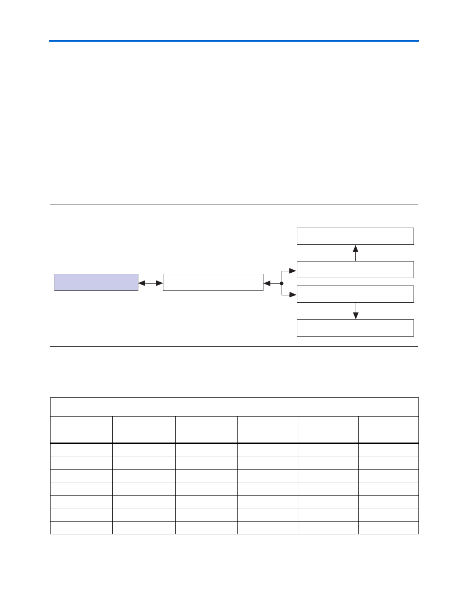
Figure 4–2
shows the DDR2 SDRAM memory termination
connections for the data, data strobe, and data mask pins. The on-board
DDR2 SDRAM memory devices share their pins on the Cyclone II device
for address and control nets, whereas the data nets are independent.
Figure 4–2. DDR2 SDRAM Memory Termination Connections
Table 4–3
shows the DDR2 SDRAM memory and termination signal
connections.
Cyclone II Banks 3 & 4
256-Mb DDR2 SDRAM Device 1
Non Fly-By Termination Resistors
256-Mb DDR2 SDRAM Device 2
Fly-By Termination Resistors
Fly-By Termination Resistors
Table 4–3. DDR2 SDRAM Memory & Terminator Signal Connections (Part 1 of 3)
DDR2 SDRAM
Signal
DDR2 SDRAM
Device 1 (U6)
DDR2 SDRAM
Device 2 (U10)
Non Fly-By
Terminator
Fly-By
Terminator
Cyclone II Pin
(U9)
DDR2_CLKEN0
K2
K2
N/A
RN11.2
D21
DDR2_CSn0
L8
L8
N/A
RN11.6
C23
DDR2_RASn
K7
K7
N/A
RN9.1
D7
DDR2_CASn
L7
L7
N/A
RN13.4
F9
DDR2_WEn
K3
K3
N/A
RN9.2
C7
DDR2_ODT
K9
K9
N/A
RN13.3
G9
DDR2_A0
M8
M8
N/A
RN13.2
A19