Block diagram – Altera Cyclone II EP2C35 PCI Development Board User Manual
Page 9
Altera Corporation
Core Version a.b.c variable
1–3
May 2005
Cyclone II EP2C35 PCI Development Board Reference Manual
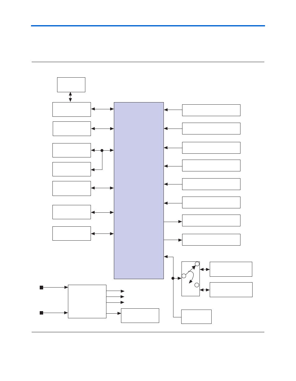
Introduction
Block Diagram
Figure 1–1
shows the board’s block diagram.
Figure 1–1. PCI Development Board, Cyclone II Edition Block Diagram
EP2C35F672
Cyclone II
Device
PCI Bus Switches
64-MByte DDR2
SDRAM Memory
Altera Daughter
Card (PROTO1)
Mictor Probe
Debug Connector
10/100 Ethernet
RS-232
JTAG Connector
High-Speed Clock Oscillator
Pushbutton Switches
DIP Switch Settings
User DIP switches
Jumpers
User LEDs
Status LEDs
Power
Regulators
External Power
Connector
Power LEDs
+3.3 V
+1.8 V
+1.2 V
PCI, PCI-X
Connector
Active Serial
Configuration
PCI Edge
Connector
+3.3V
Toggle
Switch
EPCS64 Safe Flash
Serial Programmer
EPCS64 User Flash
Serial Programmer
SMA Clock Connector
+16 V DC INPUT