Pin-outs & signal specifications, Pci & pci-x bus interfaces, Chapter 4. pin-outs & signal specifications – Altera Cyclone II EP2C35 PCI Development Board User Manual
Page 35: Introduction –1 pci & pci-x bus interfaces –1, Introduction
Altera Corporation
Core Version 4.0.0
4–1
May 2005
Preliminary
4. Pin-Outs & Signal
Specifications
Introduction
This chapter provides the following board pin-out and signal
specifications:
■
PCI & PCI-X bus interfaces
■
Memory
■
I/O
■
Configuration
■
Control & user settings
■
Altera
®
daughter card
PCI & PCI-X Bus
Interfaces
Board header J13 is a 3.3/5.0-V universal PCI connector. Board
components U13 - U17 and U20 - U24 are level converters that reduce
5.0-V PCI backplane signals to allowable 3.3-V ranges.
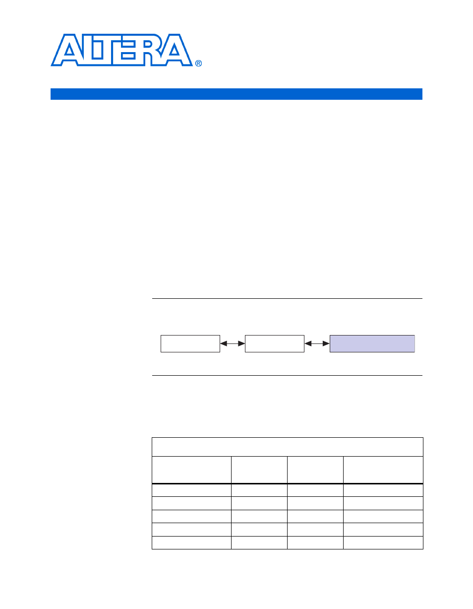
Figure 4–1
shows
PCI signal flow between the PCI connector and the Cyclone
™
II device via
the level converters.
Figure 4–1. PCI Signal Flow Using Level Converters
Table 4–1
shows the relationship between the PCI signal, PCI connector,
Cyclone II device pin, and the local signal. The level converters are not
shown.
Table 4–1. PCI Signals & Connections (Part 1 of 4)
PCI Signal
PCI Connector
(J13)
Cyclone II Pin
(U9)
Local Signal
PCI_CLK/PCIX_CLK
B16
W26/P26
LPCI_CLK
PCI_RSTn
A15
N25
LPCI_RSTn
PCI_LOCKn
B39
V22
LPCI_LOCKn
PCI_INTAn
A6
M20
LPCI_INTAn
PCI_IDSEL
A26
M25
LPCI_IDSEL
PCI Connector
Level Converters
Cyclone II Device Banks 5 & 6