Altera Stratix II GX EP2SGX90 Transceiver Signal Integrity Development Board User Manual
Page 18
2–8
Reference Manual
Altera Corporation
Stratix II GX EP2SGX90 Transceiver Signal Integrity Development Board
May 2006
Clocking Circuitry
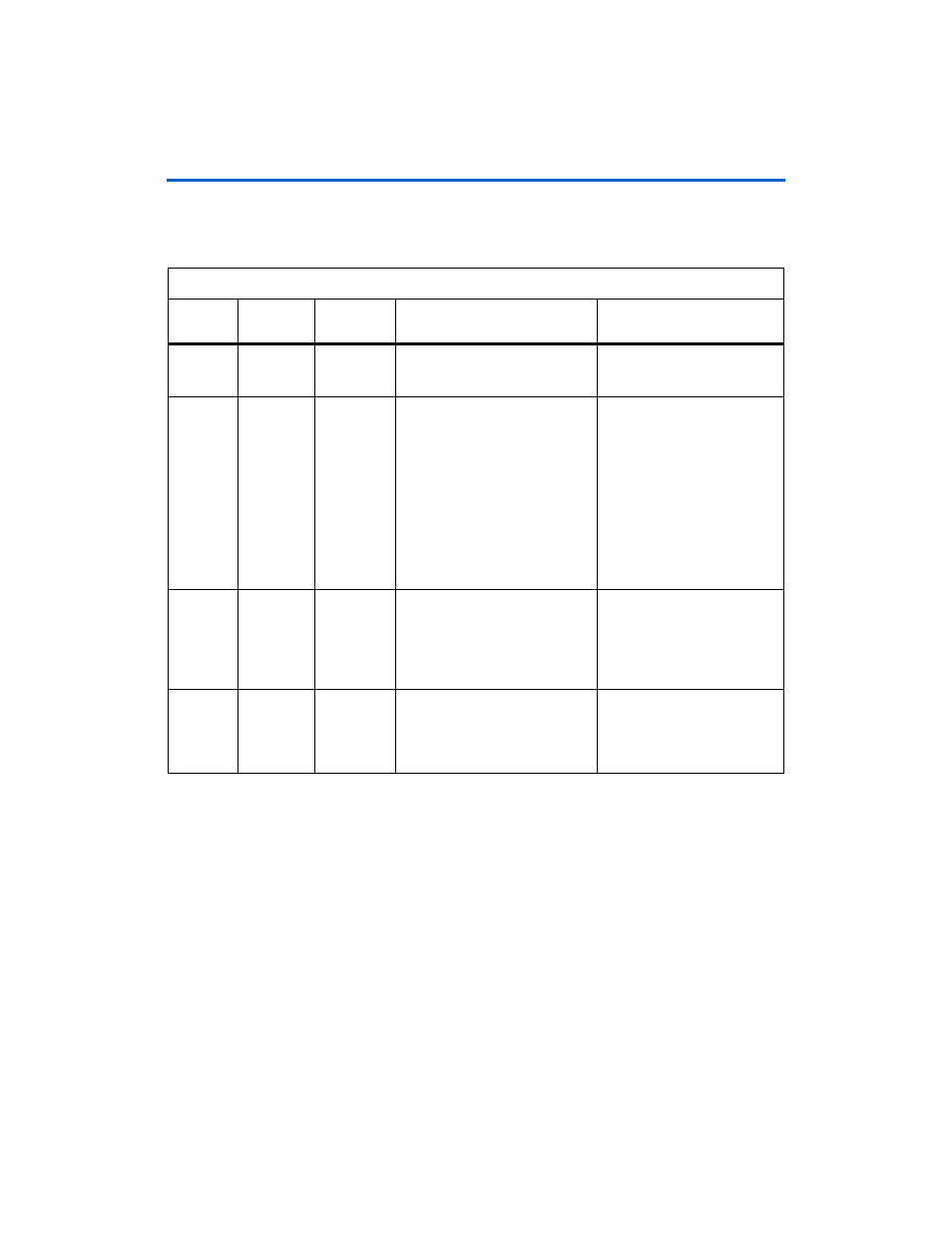
Table 2–4
lists the clocking circuitry’s board references, speeds, interface
support, and manufacturing information.
Table 2–4. Board Clocking Circuitry
Board
Reference
Speed
I/O Support
Manufacturing Information
Additional Information
U9
156.25 MHz XAUI
CEI-6G
SMD package, 3.3V, low-voltage
positive emitter coupled logic
(LVPECL) output
Supports the OIF, CEI-6G, and
XAUI protocols.
U5
25, 100,
125, and
200 MHz
PCI-Express
GbE
16-pin TSSOP package, 3.3V, and
high-speed current steering logic
(HCSL) output
Part # ICS557-03
Spread-spectrum clock
generator for PCIe clocks.
The integrated circuit system’s
(ICS) PLL uses a 25 MHz crystal
input and produces two pairs of
differential outputs at 25-MHz,
100-MHz, 125-MHz, and
200-MHz clock frequencies. The
PLL also provides spread
selection of
±25%
, -0.5
%
,
-0.75
%
, and no spread.
U7
25 MHz
Differential
I/O to
single-ended
buffer
Small outline integrated circuit
(SOIC) 8-pin package, 3.3V, and
LVDS/LVPECL/HCSL input and
LVCOMS output
Part # ICS83023
Differential I/O to LVCMOS
translator.
U8
50 MHz
General
purpose
clocking
20-pin TSSOP package,
3.3V, LVPECL/LVDS input and
LVDS output
Part # ICS8543
A 2:1 multiplexer to a 4:1
low-voltage differential signaling
(LVDS) fanout buffer.