Block diagram, Target applications, Block diagram -3 target applications -3 – Altera Stratix II GX EP2SGX90 Transceiver Signal Integrity Development Board User Manual
Page 9
Altera Corporation
Reference Manual
1–3
May 2006
Stratix II GX EP2SGX90 Transceiver Signal Integrity Development Board
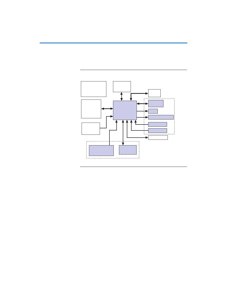
Introduction
Block Diagram
shows a functional block diagram of the Stratix II GX
EP2SGX90 transceiver signal integrity development board.
Figure 1–1. Stratix II GX EP2SGX90 Transceiver Signal Integrity Development
Board Block Diagram
Target Applications
The board is used for the following applications:
■
Demonstrating key Stratix II GX device features
■
Device qualification, e.g., jitter, pre-emphasis, equalization, and
signal integrity testing, as well as receiver sensitivity.
■
De-coupling Quartus
®
II software, transceiver architecture, and
Altera MegaWizard
®
Plug-In Manager demonstrations (supporting
devices and interfaces included)
■
Demonstrating Stratix II GX device transceiver features
■
Characterization testing of high-speed serial interfaces
■
Interoperability testing between various devices via on-board SMA
connectors
■
Power supply evaluation (on-board regulation and banana jack
options)
Po
w
er S
u
pply
Management Block
w
ith S
w
itching &
Linear Reg
u
lators
Thermal
Management
Block
Acti
v
e Serial
Config
u
ration Using
EPCS64 De
v
ice
JTAG
Config
u
ration
SMA
Connectors
for High-Speed
Interfaces
Clock
Management
Unit
USB
Interface
De
bu
gging
Header
General
User
Interface
Block
FPGA
Configuation
Block
LEDs
7-Segment Displays
Flash Memory
Stratix II GX
De
v
ice
P
u
sh B
u
ttons
DIP S
w
itches