Yaskawa 1000 Series Drive Option - Profibus-DP Technical Manual User Manual
Page 21
7 Option Data and I/O Maps
YASKAWA ELECTRIC
SIEP C730600 42B 1000-Series Option SI-P3 Technical Manual
21
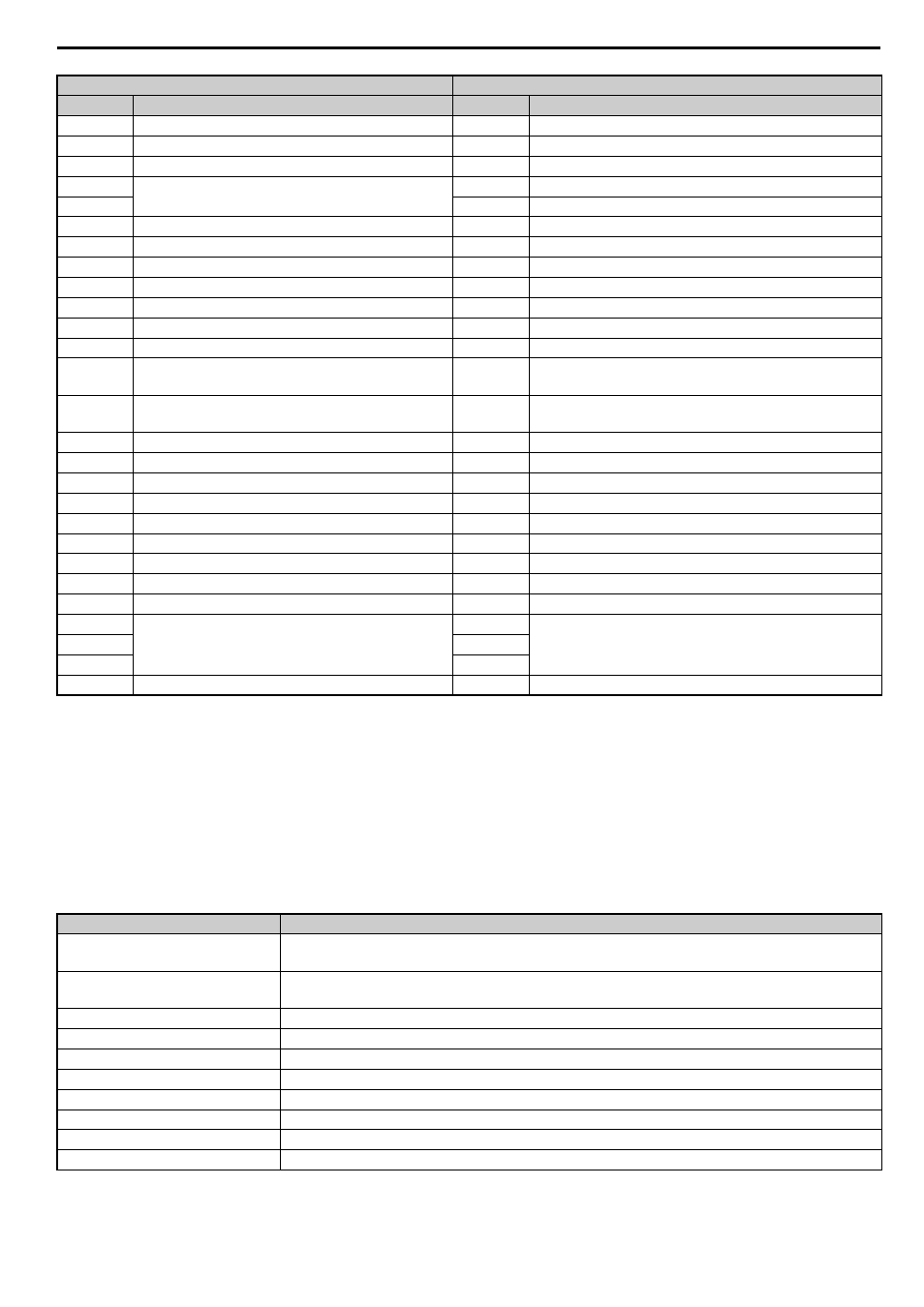
Table 11 Operation Command
5
Torque Reference Low Byte
5
Torque Reference Monitor Low Byte
6
Torque Compensation High Byte
6
Speed Detection PG Pulse Count 1 High Byte
7
Torque Compensation Low Byte
7
Speed Detection PG Pulse Count 1 Low Byte
8
Reserved
8
Frequency Reference High Byte
9
9
Frequency Reference Low Byte
10
Analog Output Channel 1 High Byte
10
Output Frequency High Byte
11
Analog Output Channel 1 Low Byte
11
Output Frequency Low Byte
12
Analog Output Channel 2 High Byte
12
13
Analog Output Channel 2 Low Byte
13
Output Current Low Byte
14
Digital Output High Byte
14
Analog Input Channel 1 High Byte
15
Digital Output Low Byte
15
Analog Input Channel 1 Low Byte
16
MEMOBUS/Modbus Function Code
16
MEMOBUS/Modbus Function Code
17
MEMOBUS/Modbus Starting Register Address High
Byte
17
MEMOBUS/Modbus Starting Register Address High Byte
18
MEMOBUS/Modbus Starting Register Address Low
Byte
18
MEMOBUS/Modbus Starting Register Address Low Byte
19
MEMOBUS/Modbus Number of Data
19
MEMOBUS/Modbus Number of Data
20
MEMOBUS/Modbus Data 1 High Byte
20
MEMOBUS/Modbus Data 1 High Byte
21
MEMOBUS/Modbus Data 1 Low Byte
21
MEMOBUS/Modbus Data 1 Low Byte
22
MEMOBUS/Modbus Data 2 High Byte
22
MEMOBUS/Modbus Data 2 High Byte
23
MEMOBUS/Modbus Data 2 Low Byte
23
MEMOBUS/Modbus Data 2 Low Byte
24
MEMOBUS/Modbus Data 3 High Byte
24
MEMOBUS/Modbus Data 3 High Byte
25
MEMOBUS/Modbus Data 3 Low Byte
25
MEMOBUS/Modbus Data 3 Low Byte
26
MEMOBUS/Modbus Data 4 High Byte
26
MEMOBUS/Modbus Data 4 High Byte
27
MEMOBUS/Modbus Data 4 Low Byte
27
MEMOBUS/Modbus Data 4 Low Byte
28
Reserved
28
Reserved
29
29
30
30
31
Handshaking Register
31
Handshaking Register
<1> Enabled in CLV, AOLV/PM, and CLV/PM control modes (A1-02 = 3, 6, or 7).
<2> Set when network communication is designated as the source of the torque limit and torque reference (F6-06 = 1).When enabled, d5-01
determines whether the value is read as the torque limit value (d5-01 = 0) or read as the torque reference value (d5-01 = 1). In CLV/PM, this
value is read as the torque limit.
<3> To select drive analog output channel for communications, set H4-01 (Multi-Function Analog Output Terminal FM) and H4-04 (Multi-
Function Analog Output Terminal AM) to 000 (through-mode).
<4> Drive digital output ON/OFF during communications, set H2-01 (Terminal M1, M2 and MC Function Selection (relay)), H2-02 (Terminal P1
Function Selection (open-collector)), and H2-03 (Terminal P2 Function Selection (open-collector)) to F (through-mode).
<5> Unit depends on the setting of o1-03 (Digital Operator Display Scaling). Input data is 0 when the drive is set for V/f Control or OLV/PM.
<6> Not possible when using V/f control, V/f with PG, or OLV/PM (A1-02 = 0, 1, or 5).
<7> Data is displayed in units of 0.01 A for drives 7.5 kW and smaller, and in units of 0.1 A for drives 11 kW and larger. This convention is the same
regardless of drive duty mode selection.
Command Signal
Description
0
H5-12 = 0: Forward Run/Stop, 1: FRUN
H5-12 = 1: Run/Stop, 1: RUN
1
H5-12 = 0: Reverse Run/Stop, 1: RRUN
H5-12 = 1: Forward/Reverse, 1: REV
2
Multi-function digital input command 3
3
Multi-function digital input command 4
4
Multi-function digital input command 5
5
Multi-function digital input command 6
6
Multi-function digital input command 7
7
Multi-function digital input command 8
8
External Fault, 1: Fault (EF0)
9
Fault Reset, 1: Fault Reset
Output (Master Device to Drive)
Input (Drive to Master Device)
Byte
Description
Byte
Description