Below is a block diagram of the clock circuitry, Figure 6 - clock circuitry block diagram – Sundance SMT702 User Manual
Page 21
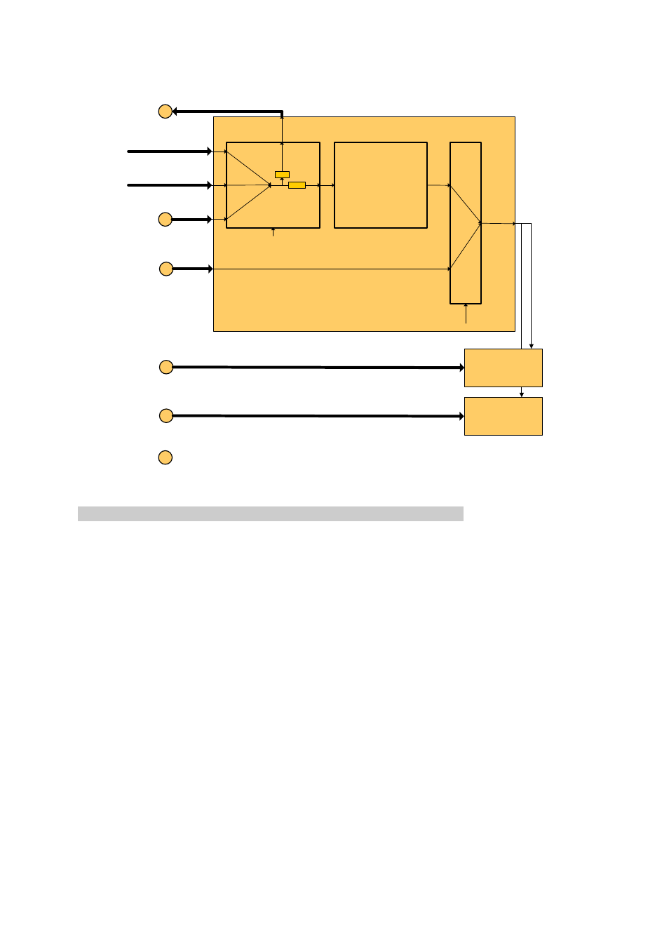
Below is a block diagram of the clock circuitry.
#2
#1
ADCA (8-bit,
3GSPS)
ADC083000
National Semiconductor
#3
Ext Clk
#4
Ext Ref
Clock Distribution LMX2531
National Semiconductor
ADCB (8-bit,
3GSPS)
ADC083000
National Semiconductor
Note that all blocks are control by the Register Block. Command are
received from the PXIe bus and decoded.
#x
SMA connector on
the front panel
PXIe Ref (100MHz)
(back-plane)
PXIe Ref (10MHz)
(back-plane)
#5
Ref Out
Reference Clock Selection
c_RF_CLK_SEL[1:0]
“10
”
“01”
“0
0”
c_REF_CLK_ON
BOARD_DIV
c_REF_CLK_
OUT_DIV
5-80
MHz
Fixed on-board clock generator
(1.5GHz or half of it)
LMX2531
750 or 1500
MHz
LMX2531
500-1500
MHz
c_CLK_SOURCE_SEL
500-1500
MHz
“0
”
“1
”
Figure 6 - Clock circuitry Block Diagram.
4.2.6
Data (samples) path / Data capture
This section details how samples from the ADCs are being captured and stored. By
default and after a power-up or reset operation, all interfaces are in reset state. The
only exception is the PXI/Express Interface. Relevant interface should first be taken
out of the initial reset state.
The next step is to program both ADCs and the clock generator and make sure it
locked to a reference signal. This is not needed in case of using an external
sampling clock. An ADC calibration cycle can be run. ADCs are then ready to output
samples and a clock to the FPGA.
Here are the details of the following step. One Xilinx DCM per ADC clock is used
inside the FPGA to ensure a good capture of data. The status of these DCMs should
be checked to make sure they are ‘locked’. They are available in the Global Control
Register. After being latched, samples go through a multiplexer to be pipelined and
then stored into the DDR2 memory available on the board. The DDR2 interface uses
some Xilinx specific blocks, such as idelays, DCMs and Phy, which have to be
‘locked’ and ‘ready’ as well. These have to be checked the same way, using the bits
available from the Global Control Register.
Each ADC is being dedicated a DDR2 Memory bank, which can be seen as a Fifo.
Both Fifos have status bits to check whether they are empty or full (bit available
from Global Control Register). Each Fifo is connected to a DMA channel. DMA
channel are implemented as Xlinks.