2 set control register – 0x10 (write) – Sundance SMT702 User Manual
Page 34
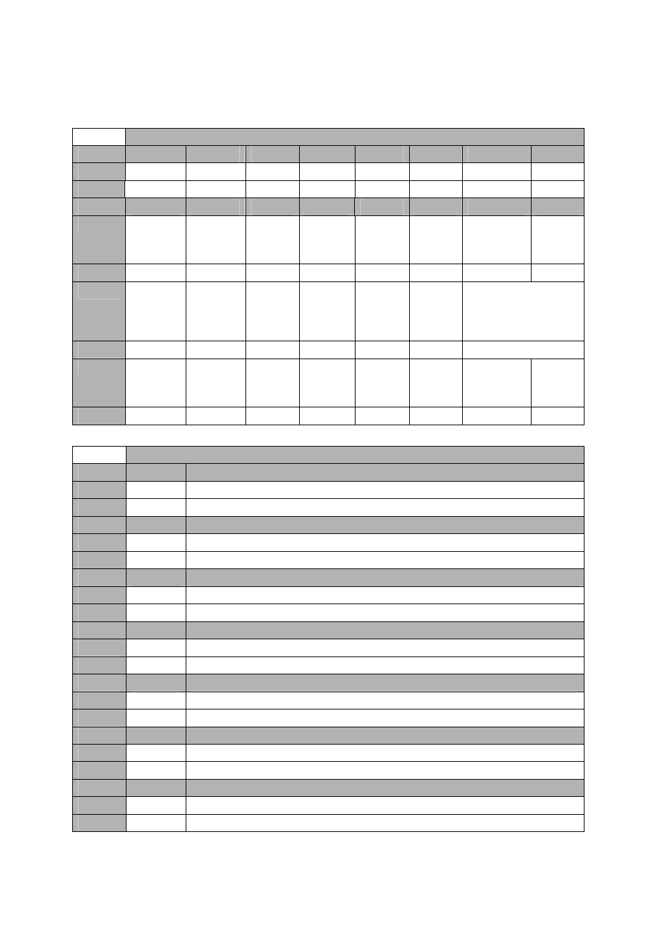
4.3.1.2.2
Set Control Register – 0x10 (write).
Offset 0x0400 -
Reset Register – 0x10 (write)
Byte
Bit 7
Bit 6
Bit 5
Bit 4
Bit 3
Bit 2
Bit 1
Bit 0
3
Default
‘0’
‘0’
‘0’
‘0’
‘0’
‘0’
‘0’
‘0’
Byte
Bit 7
Bit 6
Bit 5
Bit 4
Bit 3
Bit 2
Bit 1
Bit 0
2
System
Monitor
Reset
Soft Reset
SHB2
Reset
SHB1
Reset
DDR2
Reset
DDR2
ChA&B
Read
Enable
External
Trigger
Selection
DDR2
Capture
enable
Default
‘0’
‘1’
‘0’
‘0’
‘0’
‘0’
‘0’
‘0’
1
DCM Reset
ADC
Calibration
request
(auto-
clears)
Reference
Clock
OnBoard
Divider
Reference
Clock Out
Divider
Ref
Clock
Circuitry
Reset
Ref Clock Selection
Default
‘0’
‘0’
‘0’
‘0’
‘0’
‘1’
‘00’
0
Sampling
Clock
Selection
Source
CLOCK
Power
Supplies
Enable
ADCB
Power
Supplies
Enable
ADCA
Power
Supplies
Enable
ADC
Reset
Clock
Update
(auto-
clears)
ADCB
Update
(auto-clear)
ADCA
Update
(auto-
clears)
Default
‘0’
‘0’
‘0’
‘0’
‘1’
‘0’
‘0’
‘0’
Offset 0x0400 -
Reset Register – 0x10 (write)
Setting
Bit 0
Description – ADCA Update (Auto-Clears)
0
0
Normal Mode of Operation
1
1
All Current ADCA Register are passed from the FPGA to the ADCA Chip
Setting
Bit 1
Description – ADCB Update (Auto-Clears)
0
0
Normal Mode of Operation
1
1
All Current ADCB Register are passed from the FPGA to the ADCB Chip
Setting
Bit 2
Description – Clock Update (Auto-Clears)
0
0
Normal Mode of Operation
1
1
All Current Clock Register are passed from the FPGA to the Clock Chip
Setting
Bit 3
Description – ADC Reset (Does not auto-clear)
0
0
Normal Mode of Operation.
1
1
ADCs kept in Reset (Default).
Setting
Bit 4
Description – ADCA Power Supplies Enable
0
0
ADCA is not powered.
1
1
Normal Mode of Operation – ADCA under power.
Setting
Bit 5
Description – ADCB Power Supplies Enable
0
0
ADCB is not powered.
1
1
Normal Mode of Operation – ADCB under power.
Setting
Bit 6
Description – CLOCK Power Supplies Enable
0
0
CLOCK circuitry is not powered.
1
1
Normal Mode of Operation – CLOCK under power.