Sundance SMT702 User Manual
Page 45
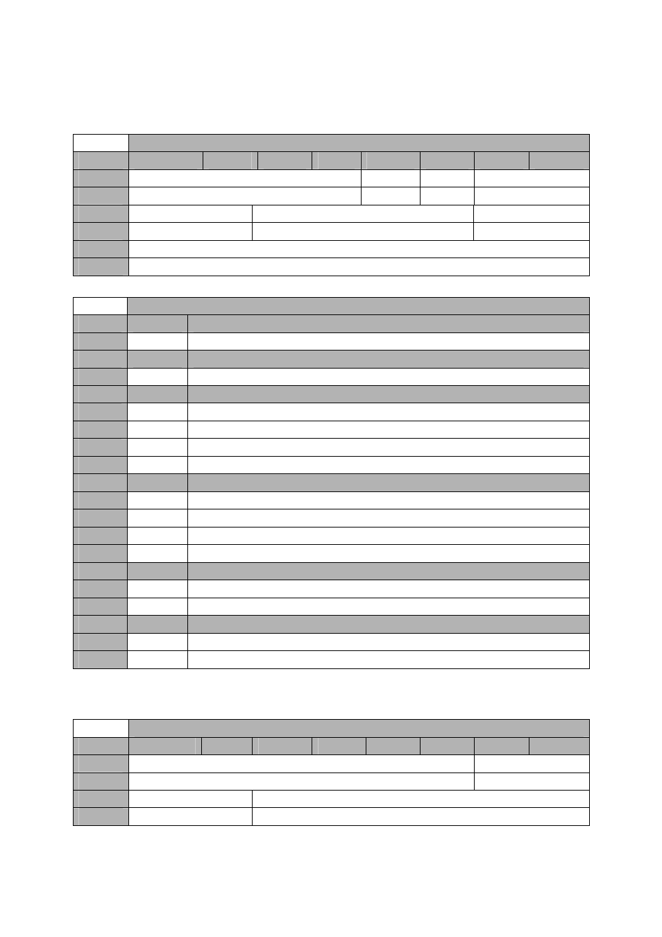
4.3.1.2.21
Frequency Synthesizer (LMX2531) Register R3 – 0xCC
(write and read).
Offset 0x0400 -
Frequency Synthesizer (LMX2531) Register R3 – 0xCC (write and read)
Byte
Bit 7
Bit 6
Bit 5
Bit 4
Bit 3
Bit 2
Bit 1
Bit 0
2
Reserved
DIV2
FDM
DITHER[1:0]
Default
‘0000’
‘0’
‘0’
‘00’
1
ORDER[1:0]
FoLD[3:0]=’0000’
DEN[21:12]
Default
‘00’
‘0000’
‘00’
0
DEN[21:12]
Default
‘00000000’
Offset 0x0400 -
Frequency Synthesizer (LMX2531) Register R3 – 0xCC (write and read)
Setting
Bit 9-0
Fractional Denominator DEN[21:12]
0
0
Value between 0 (all 0s) and 4194303 (all 1s)
Setting
Bit 13-10
Multiplexed Output for Ftest/LD pin FoLD[3:0]
0
0x0
Ftest/LD pin not used on the SMT702 – Set Register to 0x0
Setting
Bit 15-14
Order of Delta Sigma modulator ORDER[1:0]
0
0x0
Fourth
1
0x1
Reset Modulator (all fractions are ignored)
2
0x2
Second
3
0x3
Third
Setting
Bit 17-16
Dithering DITHER[1:0]
0
0x0
Weak dithering
1
0x1
Reserved
2
0x2
Strong Dithering
3
0x3
Dithering Disabled
Setting
Bit 18
Fractional Denominator Mode FDM
0
0x0
Only 12 LSBs of the fractional numerator and denominator are considered
1
0x1
Only the 10 MSBs of the fractional numerator and denominator are considered
Setting
Bit 19
Divide By 2 option DIV2
0
0x0
VCO output frequency not divided by 2
1
0x1
VCO output frequency divided by 2
4.3.1.2.22
Frequency Synthesizer (LMX2531) Register R4 – 0xD0
(write and read).
Offset 0x0400 -
Frequency Synthesizer (LMX2531) Register R4 – 0xD0 (write and read)
Byte
Bit 7
Bit 6
Bit 5
Bit 4
Bit 3
Bit 2
Bit 1
Bit 0
2
Reserved
ICPFL[3:0]
Default
‘000000’
‘00’
1
ICPFL[3:0]
TOC[13:0]
Default
‘00’
‘000000’