Altera Stratix IV GX FPGA Development Board User Manual
Page 31
Chapter 2: Board Components
2–23
Clock Circuitry
November 2010
Altera Corporation
Stratix IV GX FPGA Development Board, 530 Edition Reference Manual
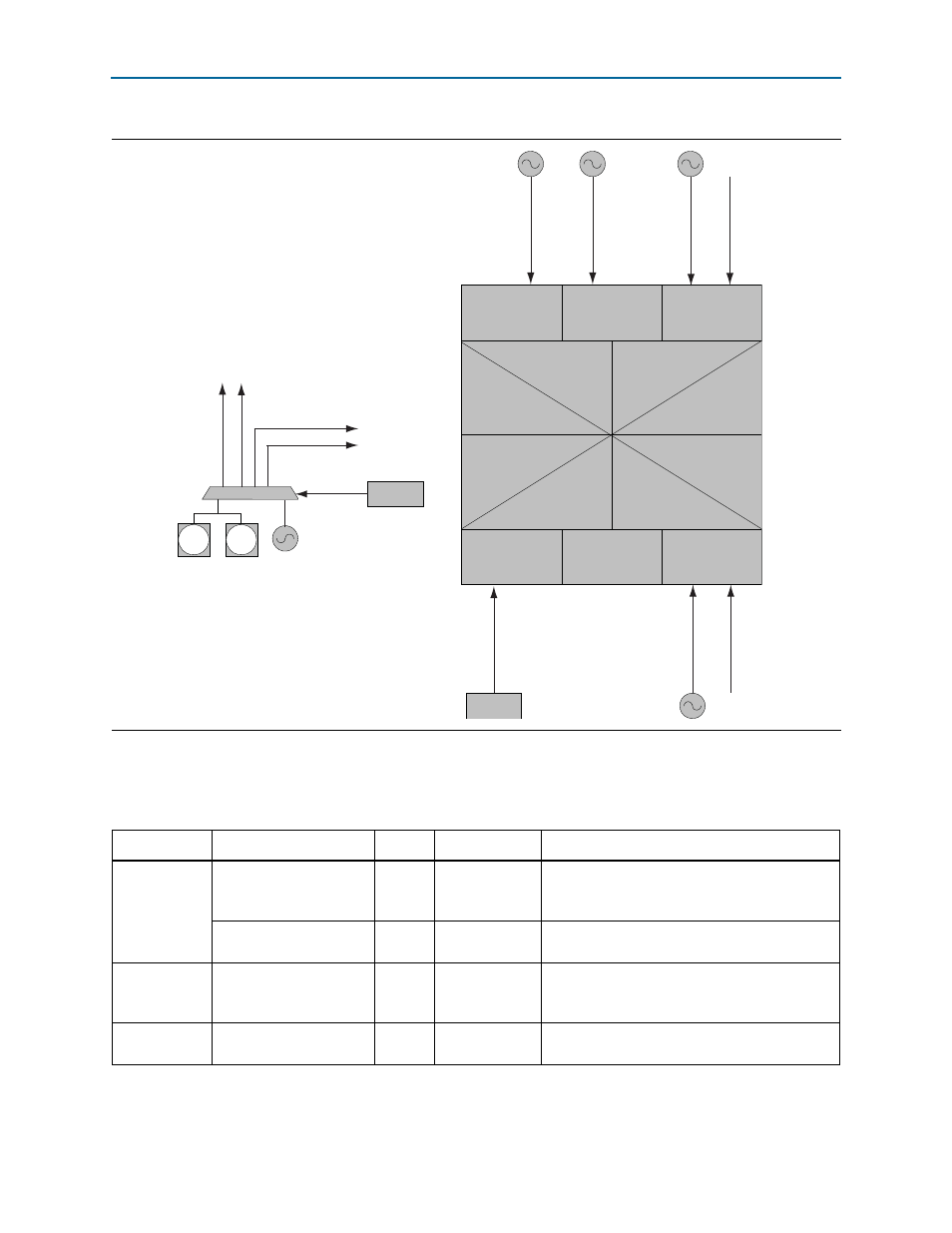
shows the external clock inputs for the Stratix IV GX FPGA Development
Board, 530 Edition.
Figure 2–7. Stratix IV GX FPGA Development Board, 530 Edition Transceiver Reference Clock Inputs
B1
B2
B3
B4
B6
B5
B8
B7
QL0
QL1
QL2
RE
F
C
LK
_L0p
RE
F
C
LK
_L1p
PCI
E
_R
EF
CL
K_
P
RE
F
C
LK
_L2p
RE
F
C
LK
_L3p
RE
F
C
LK
_L4p
RE
F
C
LK
_L5p
CLK
_155_P
CLKINLT
_100_P
LV
DS
, O
C
T
100
Ω
LVPEC
L,
O
C
T
1
00
Ω
H
C
S
L, N
O
OC
T
CLK
_125_P
CLK
INRT
_100_P
LV
DS
, O
C
T
100
Ω
LV
DS
, O
C
T
100
Ω
CLK
_156_P
LV
DS
, O
C
T
100
Ω
CLK
_148_P
LV
DS
, O
C
T
100
Ω
QR0
QR1
QR2
REF
C
LK
_R0
p
REF
C
LK
_R1
p
REF
C
LK
_R2
p
REF
C
LK
_R3
p
REF
C
LK
_R4
p
REF
C
LK
_R5
p
PCIe Edge
Connector
REFCLK INPUT
SMA
SMA
LVPECL or
Single-Ended
2-to-4 buffer
100 M*
CLK_SEL
CLK
INT
OP
_100_P
CLK
INB
OT
_100_P
CLKINRT_100_P
CLKINLT_100_P
DIPSW
SW4-5
To GPLL Clock Inputs
Right Edge
REFCLK Inputs
Left Edge
REFCLK Inputs
*The 100 MHz oscillator (X6) can be programmed
to any frequency between 20 MHz and 810 MHz
but powers up to 100 MHz using the clock control
GUI installed with the kit CD.
Table 2–20. Stratix IV GX FPGA Development Board, 530 Edition Clock Inputs (Part 1 of 2)
Source
Schematic Signal Name
Pin
I/O Standard
Description
X1
CLK_125_P0
J2
LVDS
125 MHz oscillator which drives the transceiver
reference clock input with 100
Ω on-chip
termination (OCT).
CLK_125_P1
AF34
LVDS
125 MHz oscillator which drives the global clock
input with parallel OCT.
X2
CLK_156_P
AA2
LVDS
156.25 MHz oscillator which drives the
transceiver reference clock input with 100
Ω
OCT.
X3
CLK_148_P
AL2
LVDS
148.5 MHz oscillator which drives the transceiver
reference clock input with 100
Ω OCT.