Altera Stratix IV GX FPGA Development Board User Manual
Page 32
2–24
Chapter 2: Board Components
Clock Circuitry
Stratix IV GX FPGA Development Board, 530 Edition Reference Manual
November 2010
Altera Corporation
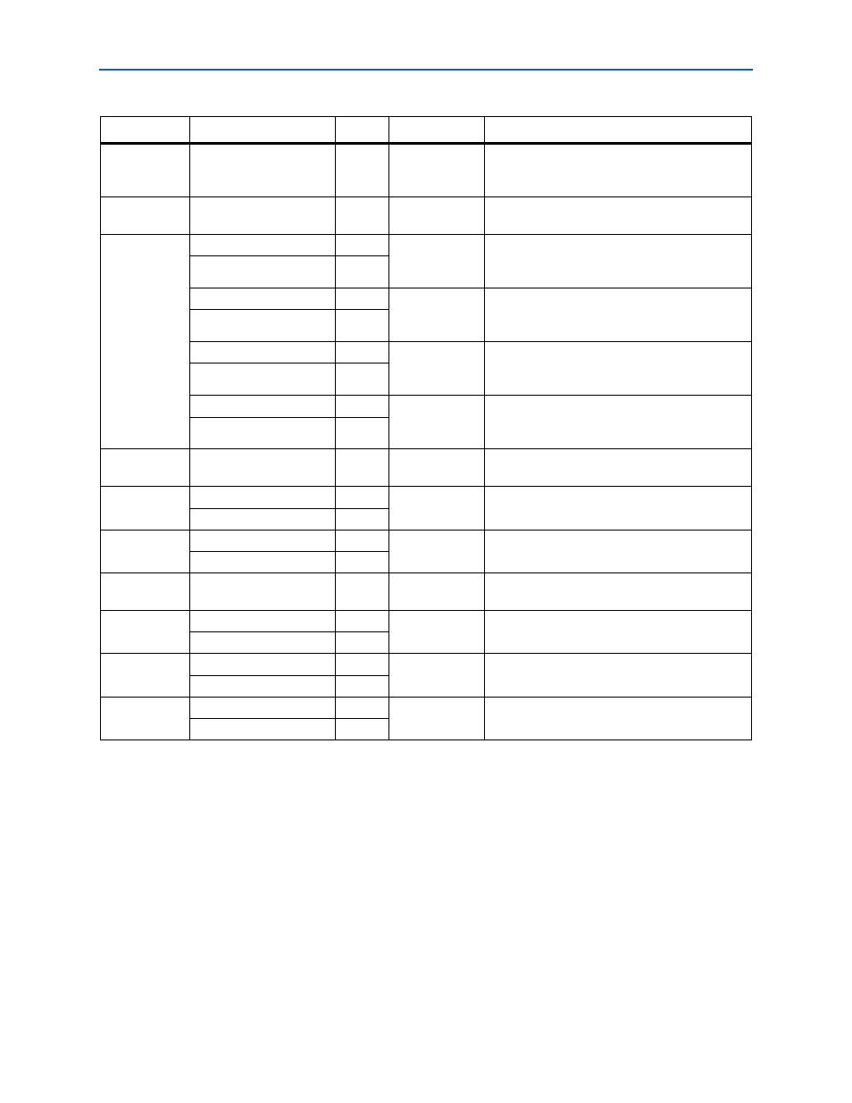
X7
CLK_155_P
J38
LVPECL
155.52 MHz oscillator which drives the
transceiver reference clock input with 100
Ω
OCT.
X8
CLKIN_50
AC34
2.5-V CMOS
50 MHz oscillator which drives the global clock
input.
SMA or X6
CLKINTOP_100_P
A21
LVDS
100 MHz programmable oscillator which drives
the fan-out buffer U50 and LVDS input to the top
edge PLL input.
CLKINTOP_100_N
A20
CLKINBOT_100_P
AV22
LVDS
100 MHz programmable oscillator which drives
the fan-out buffer U50 and LVDS input to the top
edge PLL input.
CLKINBOT_100_N
AW22
CLKINRT_100_P
G2
LVDS
100 MHz programmable oscillator which drives
the fan-out buffer U50 and LVDS to the
transceiver QR2 REFCLK input.
CLKINRT_100_N
G1
CLKINLT_100_P
G38
LVDS
100 MHz programmable oscillator which drives
the fan-out buffer U50 and LVDS to the
transceiver QR2 REFCLK input.
CLKINLT_100_N
G39
Samtec HSMC
HSMA_CLK_IN0
AB34
LVTTL
Single-ended input from the installed HSMC
cable or board.
Samtec HSMC
HSMA_CLK_IN_P1
AC6
LVDS or LVTTL
LVDS input from the installed HSMC cable or
board. Can also support two LVTTL inputs.
HSMA_CLK_IN_N1
AC5
Samtec HSMC
HSMA_CLK_IN_P2
AF6
LVDS or LVTTL
LVDS input from the installed HSMC cable or
board. Can also support two LVTTL inputs.
HSMA_CLK_IN_N2
AE5
Samtec HSMC
HSMB_CLK_IN0
AA35
LVTTL
Single-ended input from the installed HSMC
cable or board.
Samtec HSMC
HSMB_CLK_IN_P1
AB6
LVDS or LVTTL
LVDS input from the installed HSMC cable or
board. Can also support two LVTTL inputs.
HSMB_CLK_IN_N1
AA5
Samtec HSMC
HSMB_CLK_IN_P2
W6
LVDS or LVTTL
LVDS input from the installed HSMC cable or
board. Can also support two LVTTL inputs.
HSMB_CLK_IN_N2
W5
PCI Express
Edge
PCIE_REFCLK_P
AN38
HCSL
HCSL input from the PCI Express edge
connector.
PCIE_REFCLK_N
AN39
Table 2–20. Stratix IV GX FPGA Development Board, 530 Edition Clock Inputs (Part 2 of 2)
Source
Schematic Signal Name
Pin
I/O Standard
Description