Altera Stratix IV GX FPGA Development Board User Manual
Page 40
2–32
Chapter 2: Board Components
Components and Interfaces
Stratix IV GX FPGA Development Board, 530 Edition Reference Manual
November 2010
Altera Corporation
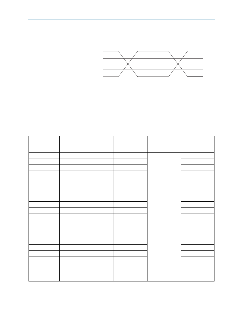
shows the PCI Express reference clock levels.
The JTAG and SMB are optional signals in the PCI Express specification. Both types of
signals are wired to the Stratix IV GX device but are not required for normal
operation. The PCI Express control DIP switch allows the presence detect grounding
to be altered to enable a ×1, ×4, or ×8 width edge connector. The PCI Express control
DIP switch does not support auto-negotiation.
summarizes the PCI
Express pin assignments. The signal names and directions are relative to the Stratix IV
GX FPGA.
Figure 2–9. PCI Express Reference Clock Levels
V
MAX
= 1.15 V
V
CROSS MAX
= 550 mV
V
CROSS MIN
= 250 mV
V
MIN
= –0.30 V
REFCLK –
REFCLK +
Table 2–34. PCI Express Pin Assignments, Schematic Signal Names, and Functions (Part 1 of 2)
Board Reference
Description
Schematic Signal
Name
I/O Standard
Stratix IV GX
Device
Pin Number
J17.A47
Add-in card transmit bus
PCIE_TX_P7
1.4-V PCML
P36
J17.A48
Add-in card transmit bus
PCIE_TX_N7
P37
J17.A43
Add-in card transmit bus
PCIE_TX_P6
T36
J17.A44
Add-in card transmit bus
PCIE_TX_N6
T37
J17.A39
Add-in card transmit bus
PCIE_TX_P5
AB36
J17.A40
Add-in card transmit bus
PCIE_TX_N5
AB37
J17.A35
Add-in card transmit bus
PCIE_TX_P4
AD36
J17.A36
Add-in card transmit bus
PCIE_TX_N4
AD37
J17.A29
Add-in card transmit bus
PCIE_TX_P3
AF36
J17.A30
Add-in card transmit bus
PCIE_TX_N3
AF37
J17.A25
Add-in card transmit bus
PCIE_TX_P2
AH36
J17.A26
Add-in card transmit bus
PCIE_TX_N2
AH37
J17.A21
Add-in card transmit bus
PCIE_TX_P1
AP36
J17.A22
Add-in card transmit bus
PCIE_TX_N1
AP37
J17.A16
Add-in card transmit bus
PCIE_TX_P0
AT36
J17.A17
Add-in card transmit bus
PCIE_TX_N0
AT37
J17.B45
Add-in card receive bus
PCIE_RX_P7
R38
J17.B46
Add-in card receive bus
PCIE_RX_N7
R39
J17.B41
Add-in card receive bus
PCIE_RX_P6
U38
J17.B42
Add-in card receive bus
PCIE_RX_N6
U39
J17.B37
Add-in card receive bus
PCIE_RX_P5
AC38