Temperature sense, Temperature sense –66 – Altera Stratix IV GX FPGA Development Board User Manual
Page 74
2–66
Chapter 2: Board Components
Power Supply
Stratix IV GX FPGA Development Board, 530 Edition Reference Manual
November 2010
Altera Corporation
lists the power measurement ADC component references and
manufacturing information.
Temperature Sense
Temperature monitoring for the Stratix IV GX FPGA die is achieved with a MAX1619
temperature sense device. The MAX1619 device connects to the MAX II CPLD
EPM2210 System Controller and the Stratix IV GX device by a 2-wire SMB interface.
The MAX 1619 device is located at address 0x1. This bus is also routed to a single
voltage and power monitor chip for the 12-V power rail at address 0x2.
The OVERTEMPn and TSENSE_ALERTn signals are driven by the MAX1619 temperature
sense device based on a programmable threshold temperature. The OVERTEMPn signal
is driven to the MAX II EPM2210 System Controller which controls OVERTEMPn. The
MAX II EPM2210 System Controller can control fan speed based on a register setting
and can also override the MAX1619 device with the FAN_FORCE_ON DIP switch to force
the fan to be on constantly at full speed. For more information on this control, refer to
the MAX II EPM2210 System Controller source code found in the development board
installation directory <install dir>\stratixIVGX_4sgx530_fpga\examples\max2
f
For more information on the development board installation directory, refer to the
6
S4VCCPT
1.5
VCCPT
Programmable power tech
7
S4VCCD_PLL
0.9
VCCD_PLL
PLL digital
8
S4VCCA_GXB
3.0
VCCA
XCVR analog TX/RX driver (mA only)
9
S4VCCIO_B5
2.5
VCCIO_B5
Bank 5 I/O power (HSMC port A)
A
S4VCCIO_B6
2.5
VCCIO_B6
Bank 6 I/O power (HSMC port B)
B
S4VCCIO_B1B2
2.5
VCCIO_B1
Bank 1 I/O power (FSM bus)
VCCIO_B2
Bank 2 I/O power (FSM bus)
C
S4VCCIO_B3A
1.8
VCCIO_B3A
Bank 3A I/O power (HDMI)
D
S4VCCIO_B3B4
1.5
VCCIO_B3
Bank 3 I/O power (DDR3BOT)
VCCIO_B4
Bank 4 I/O power (DDR3BOT)
E
S4VCC_GXB
1.1
VCCR
XCVR analog receive
VCCT
XCVR analog transmit
VCCL_GXB
XCVR clock distribution
F
—
—
—
—
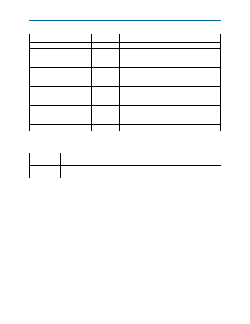
Table 2–58. Power Rail Measurements Based on the Rotary Switch Position (Part 2 of 2)
Switch
Schematic Signal Name
Voltage (V)
Device Pin
Description
Table 2–59. Power Measurement ADC Component References and Manufacturing Information
Board Reference
Description
Manufacturer
Manufacturing
Part Number
Manufacturer
Website
U1, U36
8-channel differential 24-bit ADC
Linear Technology
LTC2418CGN#PBF
U9
1-channel differential 12-bit ADC
Linear Technology
LTC4151CDD#PBF