Stratix iv gx fpga clock outputs, Stratix iv gx fpga clock outputs –25 – Altera Stratix IV GX FPGA Development Board User Manual
Page 33
Chapter 2: Board Components
2–25
Clock Circuitry
November 2010
Altera Corporation
Stratix IV GX FPGA Development Board, 530 Edition Reference Manual
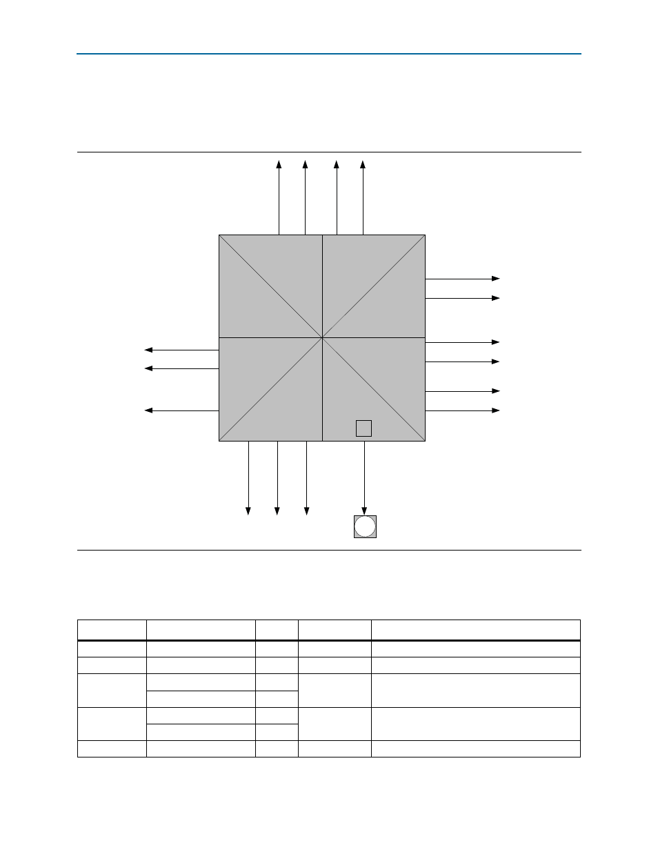
Stratix IV GX FPGA Clock Outputs
shows the Stratix IV GX FPGA Development Board, 530 Edition clock
outputs.
Table 2–21
shows the clock outputs for the Stratix IV GX FPGA Development Board,
530 Edition.
Figure 2–8. Stratix IV GX FPGA Development Board, 530 Edition Clock Outputs
B1
B2
B3
B4
B6
B5
B8
B7
SRAM
_C
LK
MA
X
2_CLK
2.
5V
, 50
Ω
OC
T
2.
5V
, 50
Ω
OC
T
SMA
PLL
L2
HS
MA
_CLK
_OUT
_P
2
LV
D
S
, N
O
OC
T
F
LA
S
H
_CLK
2.
5V
, 50
Ω
OC
T
CLKOUT
_SM
A
2.
5V
, 50
Ω
OC
T
HDMI_CLK
1.8V, 50
Ω OCT
HS
MA
_CLK
_OUT
_P
1
LV
D
S
, N
O
OC
T
HS
MB
_CLK
_OUT
_P
1
LV
D
S
, N
O
OC
T
HS
MB
_CLK
_OUT
_P
2
LV
D
S
, N
O
OC
T
DDR3BOT_CK_P
SSTL-15 Class I
DDR3BOT_CK_N
SSTL-15 Class I
DDR3TOP_CK_P
SSTL-15 Class I, 50
Ω OCT
DDR3TOP_CK_N
SSTL-15 Class I, 50
Ω OCT
QDR2_TOP0_K_P
1.5V HSTL Class I, 50
Ω OCT
QDR2_TOP0_K_N
1.5V HSTL Class I, 50
Ω OCT
QDR2_TOP1_K_P
1.5V HSTL Class I, 50
Ω OCT
QDR2_TOP1_K_N
1.5V HSTL Class I, 50
Ω OCT
Table 2–21. Stratix IV GX FPGA Development Board, 530 Edition Clock Outputs (Part 1 of 2)
Connector
Schematic Signal Name
Pin
I/O Standard
Description
SMA
CLKOUT_SMA
W33
2.5-V
FPGA CMOS output or general purpose I/O (GPIO)
Samtec HSMC
HSMA_CLK_OUT0
AM29
2.5-V
FPGA CMOS output or GPIO
Samtec HSMC
HSMA_CLK_OUT_P1
AL10
LVDS or 2.5-V
LVDS output or two 2.5-V CMOS outputs.
HSMA_CLK_OUT_N1
AM10
Samtec HSMC
HSMA_CLK_OUT_P2
AF13
LVDS or 2.5-V
LVDS output or two 2.5-V CMOS outputs.
HSMA_CLK_OUT_N2
AG13
Samtec HSMC
HSMB_CLK_OUT0
AK29
2.5-V
FPGA CMOS output or GPIO