Ssram, Ssram –58 – Altera Stratix IV GX FPGA Development Board User Manual
Page 66
2–58
Chapter 2: Board Components
Memory
Stratix IV GX FPGA Development Board, 530 Edition Reference Manual
November 2010
Altera Corporation
lists the QDRII+ top port 1 component reference and manufacturing
information.
SSRAM
The Synchronous Static Random Access Memory (SSRAM) device consists of a single
standard synchronous SRAM, providing 2 Mbyte with a 36-bit data bus. This device is
part of the shared FSM Bus, which connects to the flash memory, SSRAM, and the
MAX
II CPLD EPM2210 System Controller.
The device speed is 250 MHz single-data-rate. There is no minimum speed for this
device. The theoretical bandwidth of this 32-bit memory interface is 8.0 Gbps for
continuous bursts. The read latency for any address is two clocks, in which at
250 MHz, the latency is 10 ns and at 50 MHz, the latency is 40 ns. The write latency is
one clock.
U7.F11
Read data bus
QDR2TOP1_Q5
1.5-V HSTL Class I
G14
U7.J10
Read data bus
QDR2TOP1_Q4
H14
U7.K11
Read data bus
QDR2TOP1_Q3
K12
U7.L11
Read data bus
QDR2TOP1_Q2
J12
U7.M10
Read data bus
QDR2TOP1_Q1
K13
U7.P11
Read data bus
QDR2TOP1_Q0
J13
U7.A11
Read clock P
QDR2TOP1_CQ_P
H13
U7.A1
Read clock N
QDR2TOP1_CQ_N
L13
U7.A8
Read port select
QDR2TOP1_RPSn
F19
U7.P6
Read data valid
QDR2TOP1_QVLD
D13
U7.H1
DLL enable
QDR2TOP1_DOFFn
D20
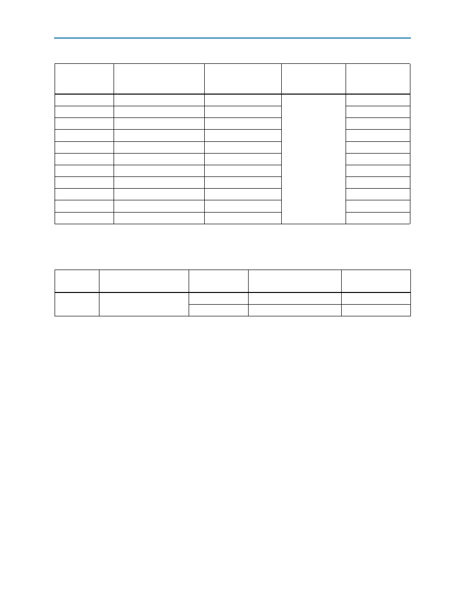
Table 2–52. QDRII+ Top Port 1 Pin Assignments, Schematic Signal Names, and Functions (Part 3 of 3)
Board Reference
Description
Schematic Signal Name
I/O Standard
Stratix IV GX
Device
Pin Number
Table 2–53. QDRII+ Top Port 1 Component Reference and Manufacturing Information
Board
Reference
Description
Manufacturer
Manufacturing
Part Number
Manufacturer
Website
U7
QDRII+, 4 M × 18, 400 MHZ
Cypress
CY7C2563KV18-400BZXC
NEC
uPD44647186AF5-E22-FQ1